Categories
Electronic Components

Process nodes and transistor density

Process nodes and transistor density

There are regular news articles published claiming that the smallest ever process node has been produced. We hear all the time about how small chips are becoming. But how can we measure this progress and does size really matter?

Moore’s Law

The concept of Moore’s Law, loosely, is that the number of transistors in a microchip increases as the size decreases. Originally, when Gordon Moore observed this in 1965, it was thought that the number of transistors would double every two years, but this rapid rate has definitely slowed.

Even so, there is still a constant increase in the number of transistors that can fit on an IC. In 1971, 6 years after the advent of Moore’s Law, there were around 2.3 thousand transistors on a single chip. This sounds like a lot, but we can now fit hundreds of millions onto one.

Nowadays, as it probably always was, it is a race between manufacturers to produce the smallest, most advanced chips. And with the advancement of manufacturing technology, the stakes are higher than ever.

Process nodes

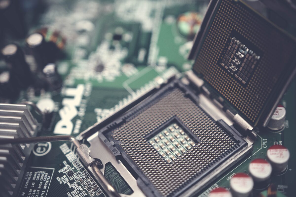
The main method of measuring electronic component progress now is through process nodes. This is the term used for the equipment used for semiconductor wafer production. It describes the minimum repeatable half-pitch (half the distance between two identical features on a chip) of a device. It seems, though, that even this node measurement is no longer accurately used, according to some sources.

Some recent node announcements come from big players in the industry, including Intel, Samsung and TSMC. Taiwan’s largest semiconductor company, TSMC, recently announced that it would be converting its 3nm process node into 1.4nm. Critics, however, were not sure how possible this would be.

Samsung also recently revealed its plans to start manufacturing 2nm process chips in 2025. Additionally, Intel is planning on producing 1.8nm chips in late 2024. Part of the process of developing smaller process nodes is changing the technology involved in production.

What is the measure of a chip?

The method of measuring chips by process nodes is not entirely accurate and can be quite ambiguous. Some people have suggested chip density within the chip would be a better indicator of advancement.

While companies compete to develop the smallest process, some companies are fitting more chips onto bigger nodes. To put it in perspective, Intel’s 7nm process has 237 million per millimetre squared. In comparison, TSMC’s 5nm chip has only 171 million per millimetre squared.

So, although certain chips may have a smaller process node, it doesn’t necessarily reflect how advanced the chip actually is. Intel often uses density to describe its chips, because that is much more beneficial to them.

It’s a process

The question is, should all chips be measured this way instead of in process nodes? If process nodes aren’t accurate to their original definition, the measurements don’t indicate of the highest power chips out there. This might be confusing to consumers when choosing a manufacturer.

It will become increasingly difficult to measure in process nodes as chips get increasingly smaller. Many manufacturers are already making plans for when they begin to measure in Angstrom rather than nanometres. If the changeover from one measurement type to another was not confusing enough, if the measurement method is inaccurate, it may get very complicated.

Apparently, though, transistor count can be just as inaccurate because there is no standard way of counting them. The number of transistors on a single chip design can vary by 33-37% which is quite substantial.

The final node

Unfortunately, there’s no definitive answer on how to measure the advancement of chips anymore. Moore’s Law is far from dead, but is very much up to interpretation these days. Those purchasing or sourcing chips will have to have their wits about them.

For those sourcing chips, contact Lantek. We can source day-to-day or hard-to-find components with ease and can guarantee our customers the best price. Get in touch via sales@lantekcorp.com or call us on 1-973-579-8100 

Categories
Electronic Components

What are GaN and SiC?

What are GaN and SiC?

Silicon will eventually go out of fashion, and companies are currently heavily investing in finding its protégé. Gallium Nitride (GaN) and Silicon Carbide (SiC) are two semiconductors that are marked as being possible replacements.

Compound semiconductors

Both materials contain more than one element, so they are given the name compound semiconductors. They are also both wide bandgap semiconductors, which means they are more durable and capable of higher performance than their predecessor Silicon (Si).

Could they replace Silicon?

SiC and GaN both have some properties that are superior to Si, and they’re more durable when it comes to higher voltages.

The bandgap of GaN is 3.2eV and SiC has a bandgap of 3.4eV, compared to Si which has a bandgap of only 1.1eV. This gives the two compounds an advantage but would be a downside when it comes to lower voltages.

Again, both GaN and SiC have a greater breakdown field strength than the current semiconductor staple, ten times better than Si. Electron mobility of the two materials, however, is drastically different from each other and from Silicon.

Main advantages of GaN

GaN can be grown by spraying a gaseous raw material onto a substrate, and one such substrate is silicon. This bypasses the need for any specialist manufacturing equipment being produced as the technology is already in place to produce Si.

The electron mobility of GaN is higher than both SiC and Si and can be manufactured at a lower cost than Si, and so produces transistors and integrated circuits with a faster switching speed and lower resistance.

There is always a downside, though, and GaN’s is the low thermal conductivity. GaN can only reach around 60% of SiC’s thermal conductivity which, although still excellent, could end up being a problem for designers.

Is SiC better?

As we’ve just mentioned, SiC has a higher thermal conductivity than its counterpart, which means it would outlast GaN at a higher heat.

SiC also has more versatility than GaN in what type of semiconductor it can become. The doping of SiC can be performed with phosphorous or nitrogen for an N-type semiconductor, or aluminium for a P-type semiconductor.

SiC is considered to be superior in terms of material quality progress, and the wafers have been produced to a bigger size than that of GaN. SiC on SiC wafers beat GaN on SiC wafers in terms of cost too.

SiC is mainly used for Schottky diodes and FET or MOSFET transistors to make converters, inverters, power supplies, battery chargers and motor control systems.

Categories
Electronic Components

US import tariffs on some Chinese components lifted

US import tariffs on some Chinese components lifted

Tariff exclusions introduced on a range of imported goods have been reinstated, easing trade and supply chain relations between China and the US.

The import tariffs, originally put in place in 2018 and 2019, were between 7.5% and 25% for the affected products. The reinstatement of exclusions became retroactively effective from October 2021 and covers approximately $370 billion worth of Chinese imports.

The previous administration granted more than 2,000 exclusions to give relief to certain industries, but most expired before the end of 2020.

Several industries were seriously affected by the original tariffs, including the electronic component market. Parts like capacitors, resistors, transistors, PCBs and many more were hit with huge tariffs, which affected the price of end products and even stopped manufacturing in some sectors.

Areas affected

Aside from components falling victim to high tariffs, medical equipment and PCBs featured in X-ray machinery were also impacted. As many of the tariffs were introduced during the pandemic there was already a heightened demand, and the US had to find products in other places, probably also facing higher costs.

PCBs and graphics cards for use in computers ended up being slapped with a hefty tariff too. The computer sector was one that experienced huge sales during the pandemic, which was one of the factors that contributed to the semiconductor shortage.

Alongside the shortage of PCBs and components, there ended up being additional backlog with tariffs being placed on other consumer electronics like phones, laptops and smartwatches.

What next?

The tariffs affecting electronic components, although high to manufacturers, were likely not as impactful for their customers. Even so, there’s a chance there will be an increase in available components and for a cheaper price, which could result in a slightly lower price for consumers as well.

Products, like the x-ray machinery, that rely on entire imported PCBs may see a larger drop in price as manufacturers can once again access cheaper circuitry.

Computer parts like the GPU might continue to be sold at an increased price, both to make up for the astronomical cost they were originally bought for, and because of continued demand. Not only are graphics cards being used for gaming computers and general use but have also had attention from the crypto and data mining market.

Material costs were already raised by the pandemic, but chances are they will remain high for a while despite the tariff exclusions brought in. Manufacturers will probably try to make up for lost time and money by keeping the costs of products high. Especially for parts such as graphics cards, this might continue for quite a while.

Thankfully, Lantek is a supplier who values its customers above all else, and will always find you the best price for your parts. So don’t delay, get in touch today for all your electronics needs. Email us at sales@lantekcorp.com.

Categories
Electronic Components

How transistors replaced vacuum tubes

How transistors replaced vacuum tubes

Electronics has come on leaps and bounds in the last 100 years and one of the most notable changes is the size of components. At the turn of the last century mechanical components were slowly being switched out for electrical ones, and an example of this switch was the vacuum tube.

A lightbulb moment

Vacuum tubes were invented in the early 1900s, and the first ones were relatively simple devices containing only an anode and a cathode. The two electrodes are inside a sealed glass or aluminium tube, then the gas inside would be removed to create a vacuum. This allowed electrons to pass between the two electrodes, working as a switch in the circuit.

Original vacuum tubes were quite large and resembled a lightbulb in appearance. They signalled a big change in computer development, as a purely electronic device replaced the previously used mechanical relays.

Aside being utilised in the field of computing, vacuum tubes were additionally used for radios, TVs, telephones, and radar equipment.

The burnout

Apart from resembling a bulb, the tubes also shared the slightly more undesirable traits. They would produce a lot of heat, which would cause the filaments to burn out and the whole component would need to be replaced.

This is because the gadget worked on a principle called thermionic emission, which needed heat to let an electrical reaction take place. Turns out having a component that might melt the rest of your circuit wasn’t the most effective approach.

The transition

Transistors came along just over 40 years later, and the vacuum tubes were slowly replaced with the solid-state alternative.

The solid-state device, so named because the electric current flows through solid semiconductor crystals instead of in a vacuum like its predecessor, could be made much smaller and did not overheat. The electronic component also acted as a switch or amplifier, so the bright star of the vacuum tube gradually burned out.

Sounds like success

Vacuum tubes are still around and have found a niche consumer base in audiophiles and hi-fi fanatics. Many amplifiers use the tubes in place of solid-state devices, and the devices have a dedicated following within the stereo community.

Although some of the materials that went into the original tubes have been replaced, mostly for safety reasons, old tubes classed as New Old Stock (NOS) are still sold and some musicians still prefer these. Despite this, modernised tubes are relatively popular and have all the familiar loveable features, like a tendency to overheat.

Don’t operate in a vacuum

Transistors are used in almost every single electronic product out there. Lantek have a huge selection of transistors and other day-to-day and obsolete components. Inquire today to find what you’re looking for at sales@lantekcorp.com or use the rapid enquiry form on our website.

Categories
Electronic Components

The History of Transistors

The History of Transistors

Transistors are a vital, ubiquitous electronic component. Their main function is to switch or amplify the electrical current in a circuit, and a modern device like a smartphone can contain between 2 and 4 billion transistors.

So that’s some modern context, but have you ever wondered when the transistor was invented? Or what it looked like?

Pre-transistor technology

Going way back to when Ohm’s Law was first discovered in 1820s, people had been aware of circuits and the flow of current. As an extension of this, there was an awareness of conductors.

Following on from this, semiconductors accompanied the birth of the AC-DC (alternating current – direct current) conversion device, the rectifier, in 1874.

Two patents were filed in the 20s and 30s for devices that would have been transistors if they had ever reached past the theoretical stage. In 1925 Julius Lilienfeld of Austria-Hungary filed a patent, but did not end up releasing any papers regarding his research on the field-effect transistor, and so his discoveries were ignored.

Again, in 1934 German physicist Oskar Heil’s patent was on a device that, by applying an electrical field, could control the current in a circuit. With only theoretical ideas, this also did not become the first field effect transistor.

The invention of transistors

The official invention of a working transistor was in 1947, and the device was announced a year later in 1948. The inventors were three physicists working at Bell Telephone Laboratories in New Jersey, USA. William Shockley, John Bardeen and Walter Brattain were part of a semiconductor research subgroup working out of the labs.

One of the first attempts they made at a transistor was Shockley’s semiconductor triode, which was made up of three electrodes, an emitter, a collector and a large low-resistance contact placed on a block of germanium. However, the semiconductor surface trapped electrons, which blocked the main channel from the effect of the external field.

Despite this initial idea not working out, the issue was solved in 1946. After spending some time looking into three-layer structures featuring a reversed and forward-biased junction, they returned to their project on field-effect devices in a year later in 1947. At the end of that year, they found that with two very close contact junctions, with one forward biased and one reverse biased, there would be a slight gain.

The first working transistor featured a strip of gold over a triangle of plastic, finely cut with a razor at the tip to create two contact points with a hair’s breadth between them and placed on top of a block of germanium.

The device was announced in June of 1948 as the transistor – a mix of the words ‘transconductance’, ‘transfer’ and ‘varistor’.

The French connection

At the same time over the water in France, two German physicists working for Compagnie des Freins et Signaux were at a similar stage in the development of a point contact device, which they went on to call the ‘transistron’ when it was released.  

Herbert Mataré and Heinrich Welker released the transistron a few months after the Bell Labs transistor was announced but was engineered completely without influence by their American counterpart due to the secrecy around the Bell project.

Where we are now

The first germanium transistors were used in computers as a replacement for their predecessor vacuum tubes, and transistor car radios were produced all within only six years of its invention.

The first transistor was made with germanium, but since the material can’t withstand heats of more than 180˚F (82.2˚C), in 1954 Bell Labs switched to silicon. Later that year Texas Instruments began mass-producing silicon transistors.

First silicon transistor made in 1954 by Bell Labs, then Texas Instruments made first commercial mass produced silicon transistor the same year. Six years later in 1960 the first in the direct bloodline of modern transistors was made, again by Bell Labs – the metal-oxide-semiconductor field-effect Transistor (MOSFET).

Between then and now, most transistor technology has been based on the MOSFET, with the size shrinking from 40 micrometres when they were first invented, to the current average being about 14 nanometres.

The latest in transistor technology is called the RibbonFET. The technology was announced by Intel in 2021, and is a transistor whose gate surrounds the channel. The tech is due to come into use in 2024 when Intel change from nanometres to, the even smaller measuring unit, Angstrom.

There is also other tech that is being developed as the years march on, including research into the use of 2D materials like graphene.

If you’re looking for electronic components, Lantek are here to help. Contact us at sales@Lantekcorp.com to order hard-to-find or obsolete electronic components. You can also use the rapid enquiry form on our website https://www.cyclops-electronics.com/

Categories
component shortage

The tech industry is bracing for a potential shortage of passive electronic components

Tech industry bracing for a potential shortage of passive electronic components

By now, everyone has heard of the global semiconductor shortage. Still, the tech industry is bracing itself for an altogether larger shortage of passive electronic components that could reduce manufacturing output across multiple categories.

Passive components do not generate energy but can store and dissipate it. They include resistors, inductors (coils), capacitors, transformers, and diodes, connecting to active elements in circuits. Passives are necessary for circuit architecture, so the shortage is bad news for the electronics industry as a whole.

The current state of the passive component shortage 

The truth is there has been a shortage of certain passive components since the coronavirus pandemic hit in 2020, particularly with multilayer ceramic capacitors (MLCCs), which can be difficult to get hold of in large quantities.

Certain diodes, transistors and resistors are also in shorter supply than they were in 2019, partly because of the pandemic and a shift in manufacturing investment for active components, which have a higher margin.

You also need to look at consumer trends (what people are buying). Smartphone and smartwatch sales are higher than ever, and smart ‘Internet of Things’ devices are growing in popularity rapidly, not to mention in availability.

These devices require a lot of passive components. For example, a typical smartphone requires over 1,000 capacitors. Cars are also huge consumers of passive components, with an electric car requiring around 22,000 MLCCs alone.

The trend for next-generation technology adoption is up across all categories, be it the Internet of Things, edge computing, semi-autonomous cars and 5G. Passive components are in more demand than ever at a time when supplies are under pressure.

Price rises are now inevitable 

The price for most passive components has risen by the largest amount in over a decade in 2021, caused by supply and demand economics and a price explosion for common materials like tin, aluminium and copper, as well as rare earth metals.

While some suppliers can afford to take a hit on profits, for most, raising prices is inevitable to ensure the viability of operations.

With higher component prices and greater shortages, it is more important than ever for companies to bolster their supply chains. Complacency is dangerous in today’s market, and no company is immune to disruption.

How to beat the passive components shortage 

The passive components shortage is likely to get worse before it gets better, but there are several ways you can bolster your supply chain:

  • Equivalents: Specifying equivalent passive components is a sound way to keep your supply chain moving. When a specific passive component isn’t available, an equivalent may be available that functions in exactly the same way.
  • Ditch outdated components: Outdated components have limited or no manufacturing output when discontinued. Upgrading to modern components that are manufactured in larger quantities can help you meet demand.
  • Partner with a global distributor: Global components distributors like us source and deliver day-to-day, shortage, hard-to-find, and obsolete electronic components. We can help keep your supply chain moving in uncertain times. Contact us today with your inquiries. 
Categories
Electronic Components Technology Transistors

The multimodal transistor (MMT) is a new design philosophy for electronics

Researchers from the University of Surrey and University of Rennes have developed a technology called the multimodal transistor (MMT), which could revolutionise electronics by simplifying circuits and increasing design freedom.

The multimodal transistor is a thin-film transistor that performs the same job as more complex circuits. The MMT sandwiches metals, insulators and semiconductors together in a package that’s considerably thinner than a normal circuit.

However, the key breakthrough with the MMT is its immunity to parasitic effects (unwanted oscillations). The MMT allows consistent, repeatable signals, increasing a transistor’s performance. This is necessary for precision circuits to function as intended and is especially useful for next-gen tech like AI and robotics.

How it works

In the image below, we can see the design of the MMT. CG1 provides the means to control the quantity of charge, while CG2 is the channel control gate. CG1 controls the current level and CG2 controls the on/off state.

This is a massive shift in transistor design because it enables far greater engineering freedom. It is a simple and elegant design, yet it is so useful. It has numerous applications in analogue computation and hardware learning.

Digital-to-analogue conversion

MOSFET transistors are one of the building blocks of modern electronics, but they are non-linear and inefficient.

In a conventional circuit, gate electrodes are used to control a transistor’s ability to pass current. The MMT works differently. Instead of using gate electrodes, it controls on/off switching independently from the amount of current that passes through. This allows the MMT to operate at a higher speed with a linear dependence between input and output. This is useful for digital-to-analogue conversion.

The breakthrough in all its glory

The MMT transforms the humble transistor into a linear device that delivers a linear dependence between input and output. It separates charge injection from conduction, a new design that achieves independent current on/off switching.

There is a profound increase in switching speed as a result of this technology, enabling engineers to develop faster electronics. Researchers estimate that the switching speed is as much as 10 times faster. Also, fewer transistors are needed, increasing the yield rate and reducing the cost to manufacture the circuit.  

Just how revolutionary the MMT will be remains to be seen. After all, this is a technology without commercialisation. It could find its way into the electronics we use on a daily basis, like our phones. The potential is for the MMT to be printable, allowing for mass production and integration into billions of electrical devices.

With devices getting smarter and digital transformation advancing at a rapid rate, the electronics industry is booming. Semiconductor foundries are at peek capacity and more electrical devices are being sold than ever. The MMT is a unique solution to a problem, and it could make manufacturing electronics cheaper.   

With this, comes a great opportunity for the MMT to replace MOSFET transistors. We can think of few other design philosophies with such wicked potential.