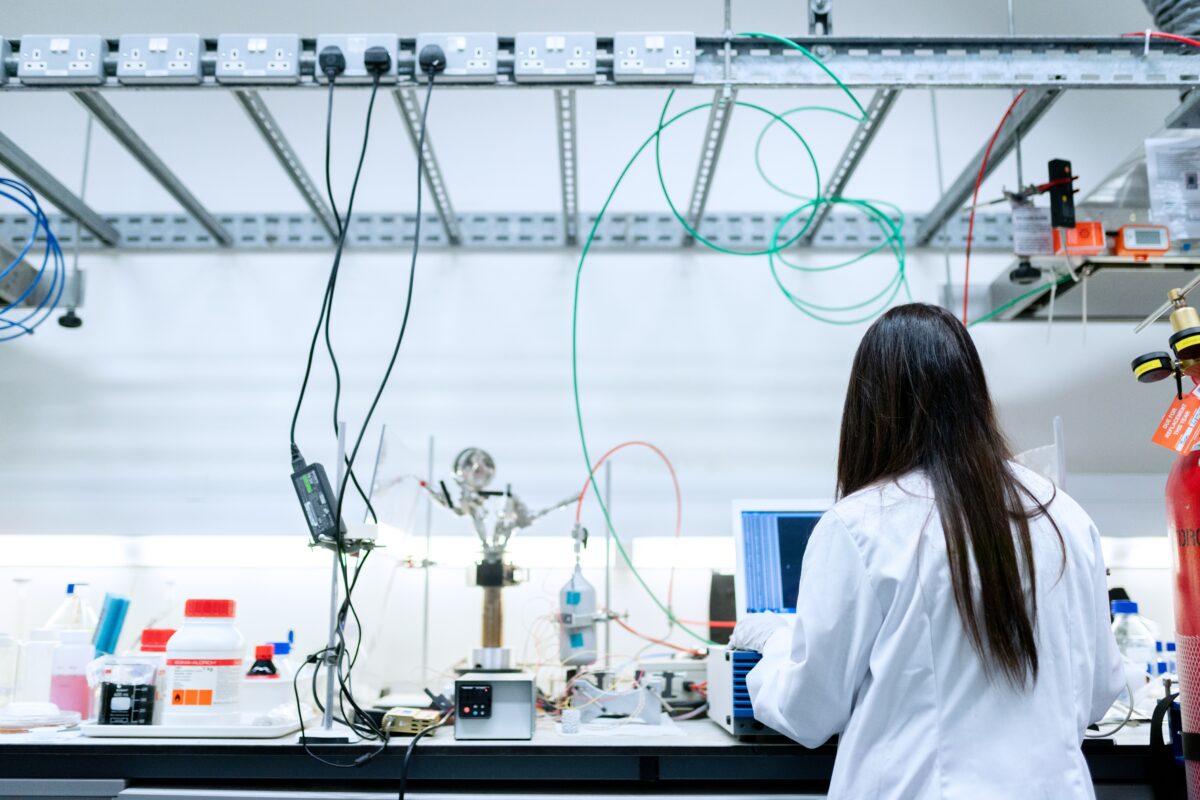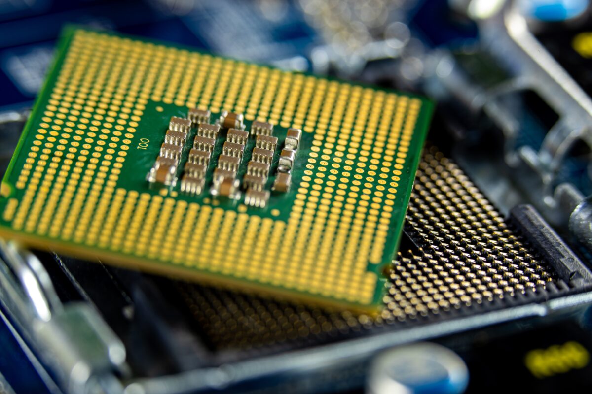

The United States has always been at the forefront of technological innovation, and the semiconductor industry is no exception. With advancements in AI, IoT, and various consumer electronics, the demand for semiconductors is skyrocketing. The US Semiconductor Ecosystem Map from the Semiconductor Industry Association (SIA), last updated on March 28, 2024, highlights key states excelling in semiconductor manufacturing and R&D. Let’s delve into the top states and understand why they are leading the charge.
Top States for Semiconductor Manufacturing
California (34 Facilities)
California is the leading state in semiconductor manufacturing, with 34 facilities. Since the 1950s, California has made innovation one of its many specialties. Shockley Semiconductor Laboratory opening in 1955 was the first semiconductor facility to open in the state and began the technology hub that would become known as Silicon Valley.
Reasons for choosing California include:
- Silicon Valley – An innovation centre, home to a high concentration of technology companies and startups.
- Established supply chains – With a recognised base comes long-existing supply chains and a sturdy infrastructure.
- Advanced technologies – Numerous modern facilities and the latest manufacturing innovations.
Arizona (28 Facilities)
One of Arizona’s first forays into semiconductors was in 1949, six years earlier than California. That year Motorola Inc. established a research lab in Phoenix, which would later become a transistor manufacturing facility.
Arizona is a popular choice because:
- Cost-effective operations – Generally lower costs of living and business operations than other states like California.
- Lessened financial burden – Alongside the lower costs, Arizona has a lot of tax incentives and subsidies to encourage businesses.
- Good climate – The dry air is ideal for semiconductor manufacturing, reducing humidity-associated risks.
Texas (17 Facilities)
Texas is known for its business-friendly environment, and is well-known for being home to some very large semiconductor companies.
Texas is a contender due to:
- Attractive business environment – The state offers lower taxes and some incentives for companies.
- Affordable – Labour, utilities, and real estate are fairly priced, making it an economical choice for companies.
- Energy – Affordable and reliable energy, a real incentive for energy-intensive semiconductor manufacturing processes.
What do they have in common?
All three states have industry clusters, leading to companies benefiting from being close to each other and sharing knowledge, suppliers, and skilled labour. Additionally, these states offer a high quality of life, which helps attract top talent. Their strategic locations ensure proximity to major consumer markets in the US and excellent connectivity for international trade.
Top States for R&D Facilities
California (87 Facilities)
With 87 R&D facilities, California is the undisputed leader in semiconductor research and development.
- University and industry: California has a strong university system with established links between industry and academia.
Texas (36 Facilities)
Again one of the top three, Texas has a significant number of R&D facilities dedicated to semiconductors.
- Educational Strengths: Texas has a number of top-tier universities with strong engineering and tech programs, feeding the industry with fresh talent and original ideas.
Massachusetts (35 Facilities)
Massachusetts is a strong competitor in semiconductor R&D, thanks to its strong educational and industry connections.
- Academic Excellence: Renowned for its world-class universities including Harvard and MIT (Massachusetts Institute of Technology), the state offers excellent opportunities for collaboration between education and industry.
Top States for Chip Design
California (64 Facilities)
In the end, California is leading the way in all three of these categories, cementing its position as a center of US semiconductor innovation.
- Education and talent: Proximity to top universities like Stanford, UC Berkeley, and Caltech fosters a strong research and talent pool, and creates a highly skilled workforce.
- Access to Capital: Significant venture capital presence supports startups and established companies, along with federal and state research grants.
Texas (22 Facilities)
Texas is another US tech hub, with a robust environment supporting semiconductor innovation.
- Business Environment: Business-friendly tax policies with no state income tax and various economic incentives, including grants and tax credits.
- Educational Institutions: Strong university system with institutions like the University of Texas and Texas A&M University contributing to R&D and providing a continuous supply of tech graduates.
Arizona (10 Facilities)
Arizona offers a stable environment for chip design, attracting numerous facilities to the state.
- Education and Workforce: Strong emphasis on tech and engineering education, with universities like Arizona State University and the University of Arizona contributing to R&D efforts.
Innovation and recognition
While California, Arizona, Texas, and Massachusetts stand out as established technology hubs, the semiconductor industry benefits from facilities and infrastructure spread across the entire USA. Many states offer generous incentives and grants to encourage new startups and foster innovation. This wide distribution of resources and support ensures that companies, regardless of location, can contribute to and thrive within the semiconductor sector.
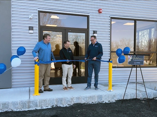
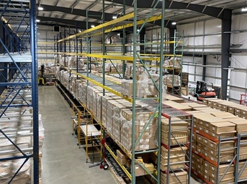
At Lantek Corporation, we are not only committed to supporting the growth and innovation of the semiconductor industry, but we are also steadfast supporters of the established semiconductor supply chain. Our expertise in sourcing both common and hard-to-find electronic components ensures that your manufacturing processes remain uninterrupted. Explore our services and discover how we can help you stay ahead in this fast-paced industry.
Contact Lantek Corporation to discover how we can support your semiconductor efforts with top-quality electronic components.