
Case Study – A switch to Efficiency and Cost-Effectiveness

The Customer
A long-standing USA-based commercial vehicle manufacturer with a history extending over a century.
The Problem: Navigating Increasing Costs and Supply Reliability
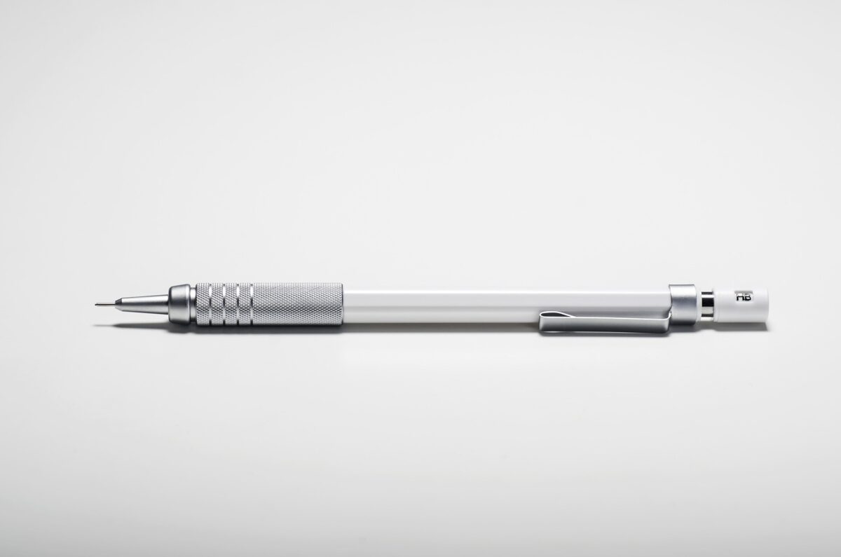
The customer was burdened by the frequent price hikes of their original switch. These increases were occurring three times annually, posing a serious financial strain.
Faced with these unsustainable costs, the customer needed an alternative that would not only be cost-effective but also ensure consistent quality and supply reliability. They required a switch that could seamlessly integrate without disrupting their manufacturing processes.
The Solution: Lantek's Tailored Sourcing Strategy
The engagement began through a trusted connection. The buyer at the customer’s end, having worked with a Senior Account Manager from Lantek in various capacities across different organizations, reached out, confident in Lantek’s ability to provide a viable solution.
Utilizing her extensive experience and understanding of the industry, Lantek’s Senior Account Manager leveraged the specifications of the existing switch to cross-reference and identify a suitable alternative. This process involved meticulous matching of PSI, size, and other critical specifications to ensure compatibility and functionality.
The Outcome: Enhanced Operational Efficiency and Cost Savings
The alternative switch sourced by Lantek not only matched the original switch in terms of fit, form, and function but also brought a more stable and predictable pricing structure. This was evidenced by only one price increase since the start of the business relationship with the new provider, in contrast to the thrice-yearly increases of the original switch.
Beyond the immediate cost savings and stability in pricing, the new switch also provided the customer with increased supply reliability. Lantek’s ability to hold stock for up to 12 months ensured that the customer had a consistent supply of the necessary components, buffering them against market fluctuations and supply chain uncertainties.
The customer expressed high satisfaction with both the quality of service and the performance of the alternative switch. Lantek’s solution was acknowledged as instrumental in addressing their primary concerns of cost and supply reliability.
Conclusion: Lantek’s Role as a Strategic Sourcing Partner
By providing a cost-effective, reliable alternative, Lantek not only aided the customer in maintaining their production efficiency but also fortified a relationship built on trust and satisfaction.
This case study serves as a testament to Lantek’s expertise in sourcing and supplying high-quality components, tailored to the specific needs of our customers. Our approach – focusing on understanding the client’s problem, strategic sourcing, and delivering customized solutions – positions us as a trusted and reliable partner in the industry, capable of tackling a variety of challenges with efficiency and effectiveness.
Lantek’s ability to provide second-source alternatives, replacements for obsolete components, and significant cost savings showcases our expertise in addressing similar challenges faced by other businesses.
For businesses seeking reliable second-source alternatives and aiming to control costs, Lantek recommends our scheduled ordering service. This service ensures fixed pricing and stock availability for up to 12 months, protecting against price increases and availability issues.
If you are facing similar challenges in your operations or seeking reliable, cost-effective sourcing solutions, get in touch today on +1 973-579-8100 or email sales@lantekcorp.com. Our team is dedicated to providing you with customized solutions that meet your unique requirements.