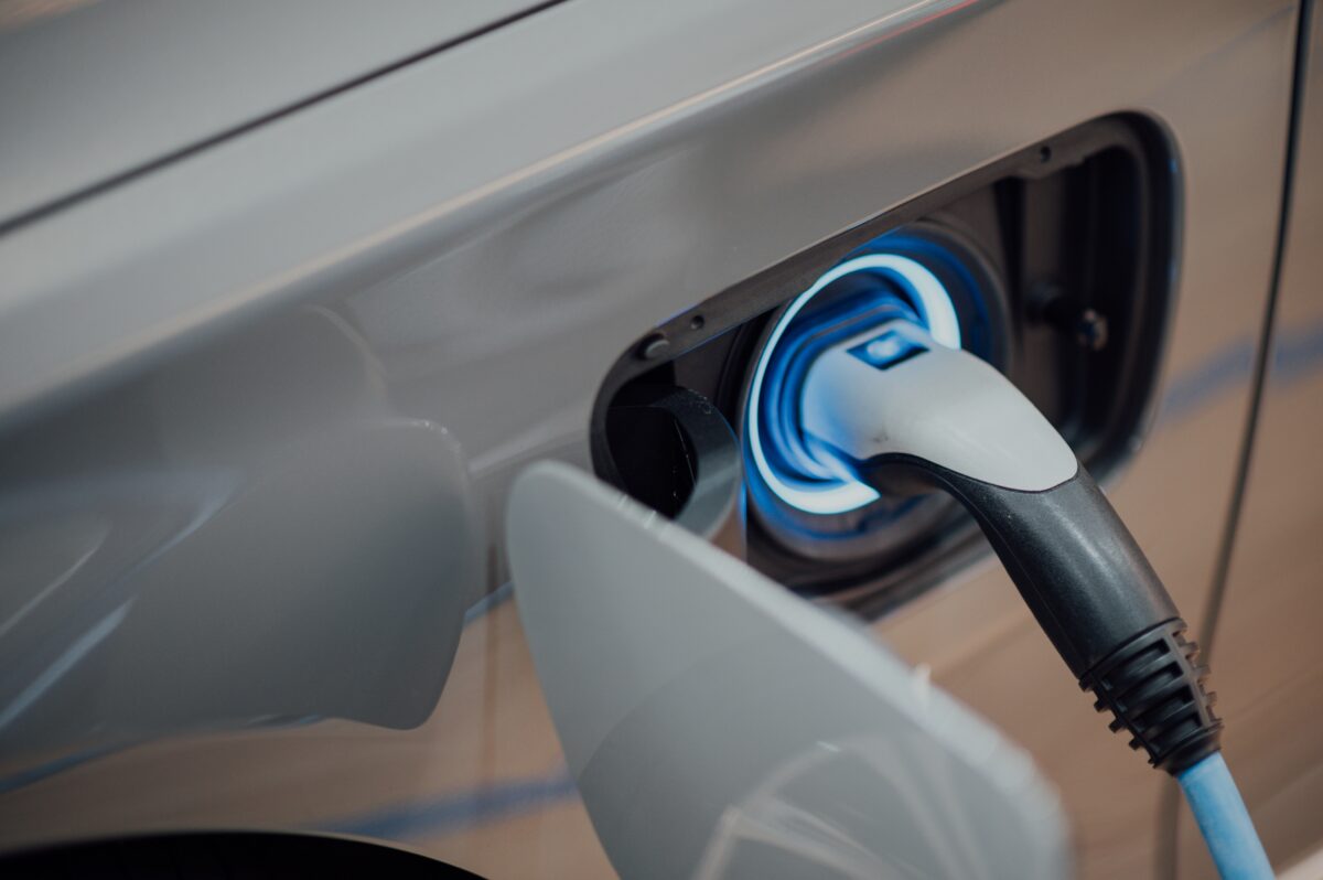
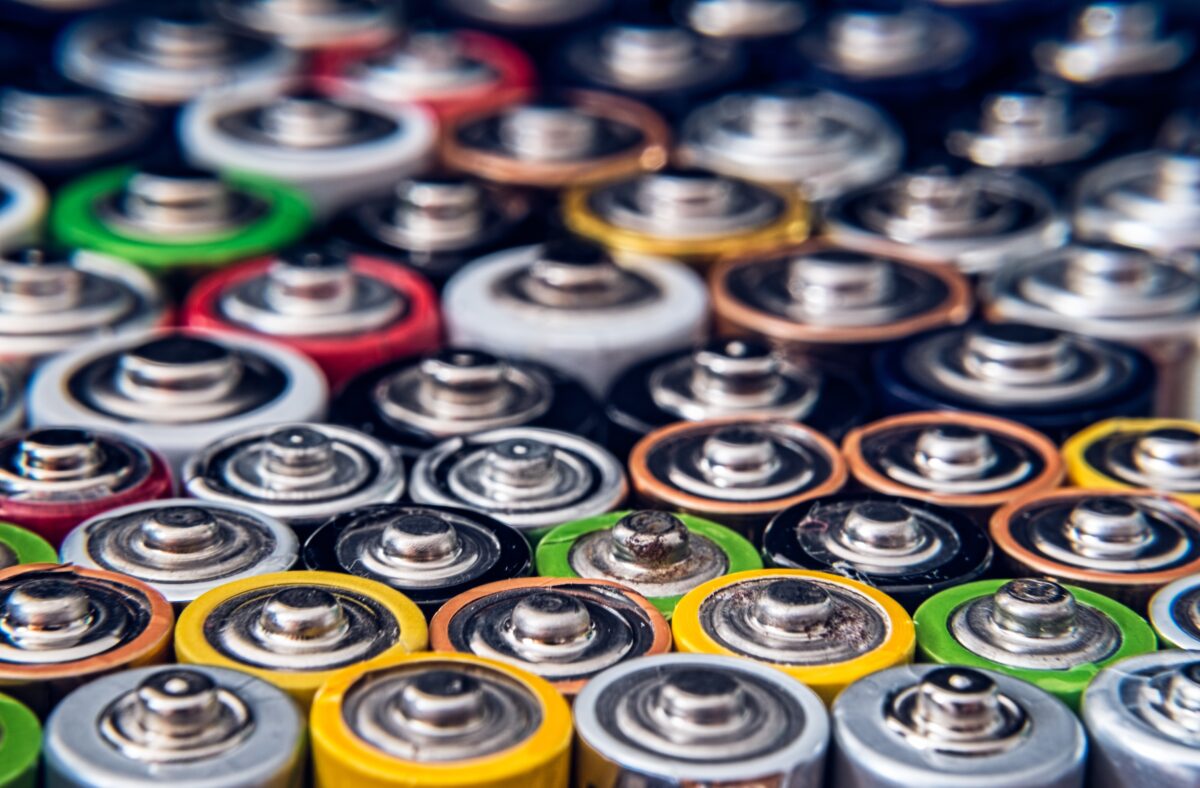
Increase in lithium battery recycling
The Department of Energy (DOE) is making further investments in lithium battery recycling.
In late February the DOE loaned battery recycling company Li-Cycle $375 million to build a plant near Rochester, New York.
This followed several other recycling companies’ announcements about lithium battery recycling facilities, including Ecobat and Redwood Materials.
The latest facility will be Li-Cycle’s fifth in North America.
Significant investment
Many facility announcements have come as production and popularity of EVs grows in the US. Not only in recycling, but also lithium battery production. Earlier this year the DOE announced a $700 million loan for a processing facility at the Rhyolite Ridge lithium deposit in Nevada.
The company in charge of the facility, Ioneer, states there will be enough lithium produced from the site to build 400,000 EVs each year.
The goals
The US is aiming for 500,000 EV chargers and 50% of all new light-duty vehicle sales being electric by 2030. They are further hoping to be a net-zero emissions economy by 2050.
Sales of EVs in the US were 630,000 in 2021, according to the International Energy Agency. This would need more than 7,560 tonnes of lithium. To reach the goals stated by the Biden Administration, 90,000 tonnes of lithium would need to be produced. This is 1700% more than the lithium currently mined in the US.
Slow and steady
A lithium mine takes between four and 20 years to begin commercial production. Although there are several projects underway in the country, there’s no telling when these might become steady sources of lithium.
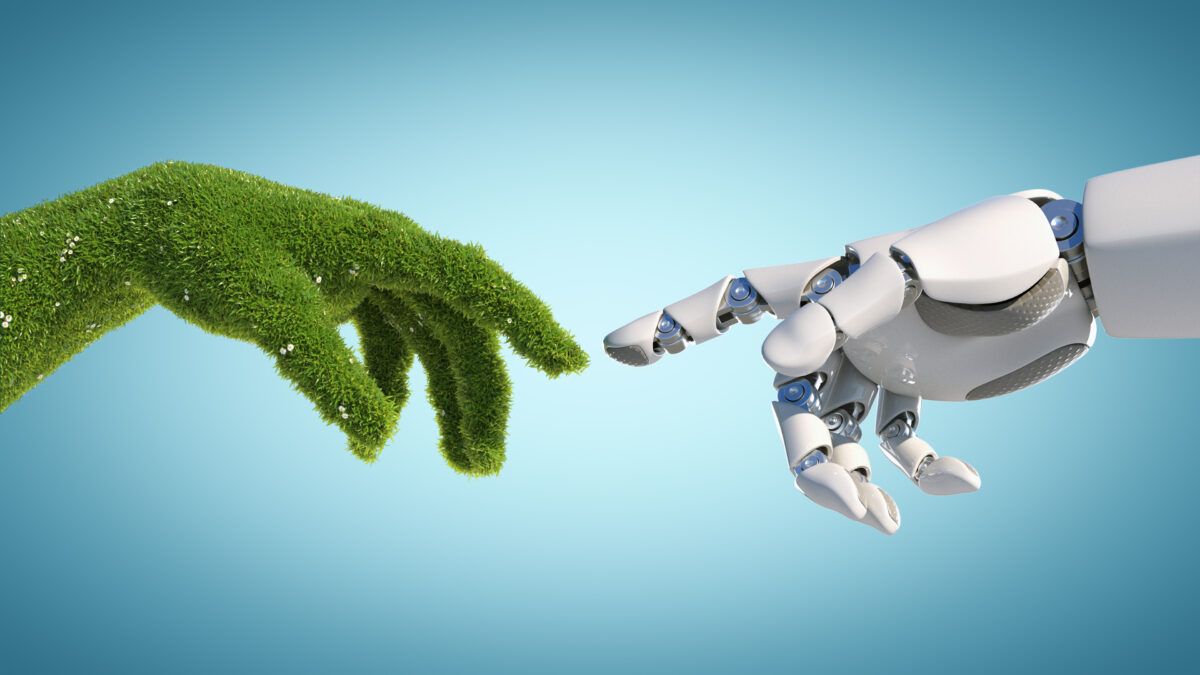
Lithium mining is a concern due to the water consumption and toxic chemicals that can leak into the environment. There are also lithium shortages predicted as soon as 2025. Recycling would make the production of lithium batteries more sustainable and potentially mitigate future shortages.
The cost of recycling these batteries can be high. There are additional risks with lithium batteries, demonstrated by the 245 fires across 4 waste facilities caused in the past. The process is pretty time-consuming too. Consequentially, the price of running safe recycling facilities is quite high.
There is hope, though, that it will be worth it in the future.
Guaranteed
Lantek is a distributor with decades of experience in the electronic components industry. Whether you’re looking for new shortage components or obsolete ones, trust Lantek to provide what you need. Call us today on 1-973-579-8100 or send us an email at sales@lantekcorp.com.