
Is it possible to make compostable PCBs?
Decades ago we wouldn’t have thought it possible to create printed circuit boards (PCBs). Now, in 2023, we’re discussing the possibility of biodegradable ones.
A research group from the Johannes Kepler University in Austria developed the biodegradable base for the PCBs. The mix consists of beech wood shavings, organise full-grain spelt flour, fine plaster (CaSO4) dust and beech wood-based inoculum.
After storing the mixture in a flat plastic box in a cupboard for a few weeks a tissue grew. The fungal fibres, called mycelium, formed a kind of soft white skin, similar to paper.
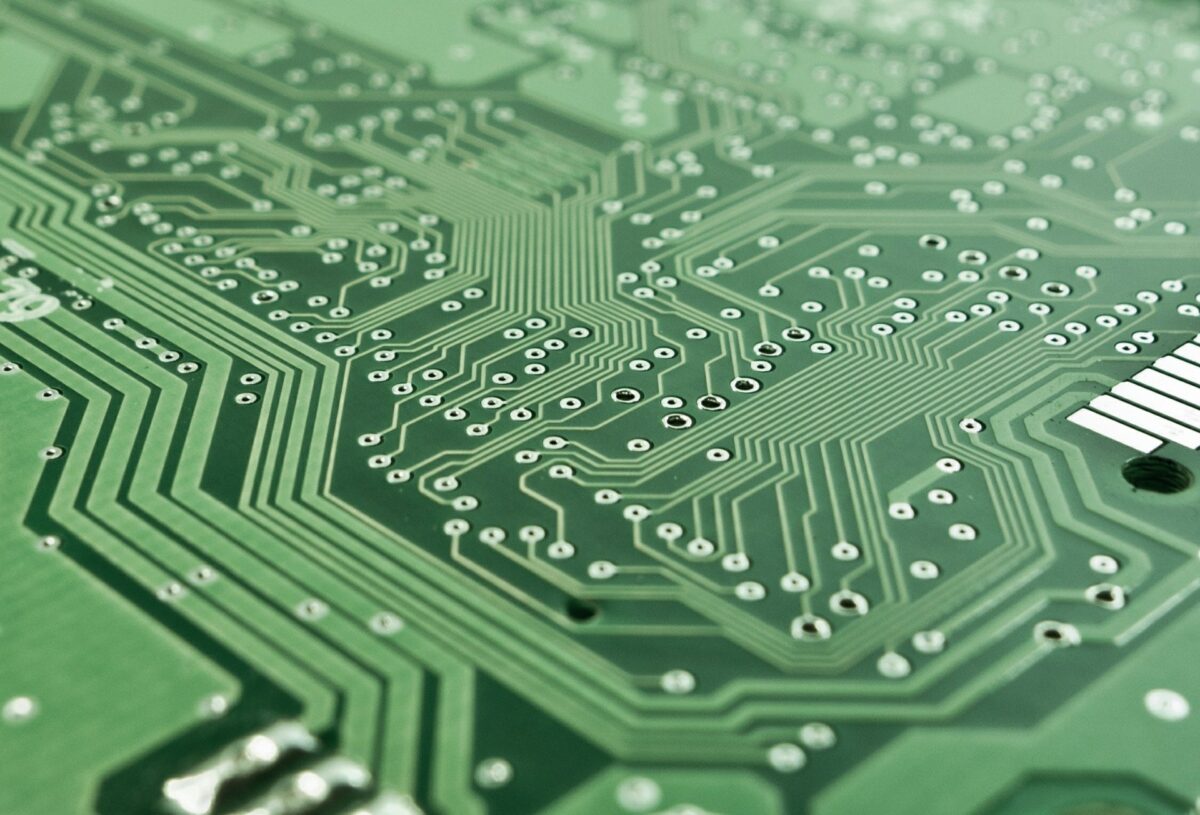
A layer of copper or gold is then vapour-deposited onto the mycelium ‘skin’. Then, a laser will cut away the metal where it’s not needed.
A ‘grow-your-own’ circuit
Storing something in a cupboard for a few weeks has significantly lower production costs than regular PCBs. It also bypasses the need for chemicals and minerals that are hazardous to the environment.
With the use of these, too, there is no need to create specialist manufacturing equipment, unlike with biopolymers. They are made from renewable raw materials like starch or milk protein, but have to use an industrial composting plant that operates at a high temperature.
These ‘skins’ can then be mounted with electronic components like a regular PCB.
The mycelium has a very strong structural integrity, while it remains thin and flexible. It has so far been able to withstand about 2,000 bending cycles, it only shows moderate resistance when folded, can insulate electrical currents and can sustain temperatures that reach 250⁰C.
Early days
So far the concept can only be used in simple electronic devices. A multi-layer circuit or more complex electronics are slightly further in the future. Even at this early development stage, though, a prototype has already been attached to a moisture sensor, a Bluetooth chip that sends the sensor signal to a laptop or smartphone, and a special battery.
In the future it is hoped that production of a smoother mycelial skin through a refined formula could increase the possibilities. It could lead to multi-layer PCBs with smaller components.
Once the circuit has been used, it can be unsoldered and put in the compost. The metal used I the conductor paths will be a biproduct left in the soil, but will be nano-particles in unharmful quantities.
Looking for a fun-guy?
Whether you’re ‘growing’ or manufacturing your PCBs, Lantek has the electronic components for you. We specialize in obsolete, hard-to-find, and day-to-day electronic components, and can source components from trusted sources globally. Contact us today to see what Lantek can do for you on sales@lantekcorp.com, or call 1-973-579-8100