Categories
Electronic Components Semiconductor

Semiconductor cleanrooms

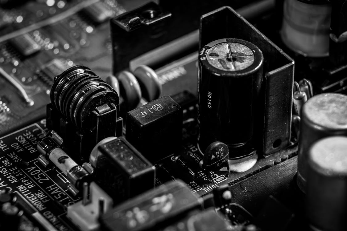
Semiconductor clean rooms

The process of making a semiconductor is a long one, and one of the essential components of the process is the cleanrooms.

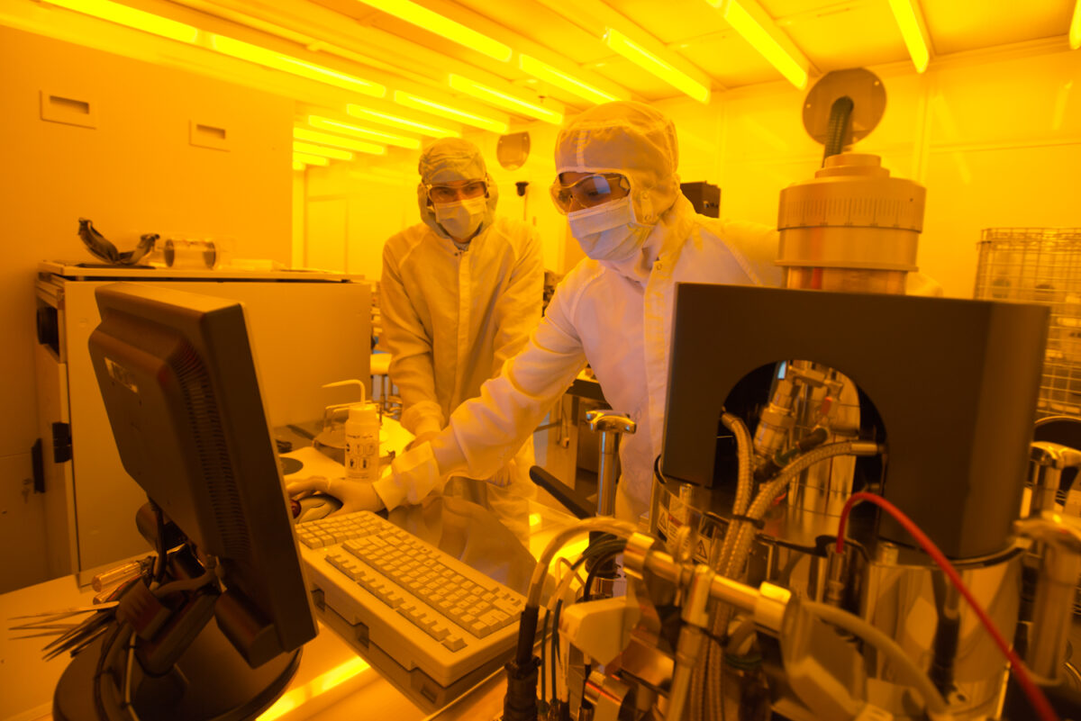
What is a cleanroom?

The semiconductor manufacturing process is a very delicate, painstaking process. Cleanrooms have really tight control over many elements,
including temperature, humidity and airflow. These things can all impact the manufacturing process.

Even a single stray particle of dust or a degree below or above the desired temperature could completely alter the semiconductor.

Heat and humidity

Heat can affect the resistance and conductivity of a semiconductor. As a semiconductor’s temperature increases, the conductivity also increases and resistance drops.

Humidity, too, can have a huge impact on the end product. According to Air Innovations, the humidity in a cleanroom should fall between 30% and 50%. These conditions are ideal for stopping bacterial growth and is comfortable for the staff working inside.

Strict regulations

There is a maximum particle count and particle size in place in cleanrooms. This is usually stipulated in ISO requirements, that cleanrooms have to comply with. Depending on the process going on in the cleanroom, the regulations could be more or less stringent.

One of the biggest risk factors to a cleanroom is the people working within it. The staff are required to wear specialist clothing to
prevent cross-contamination, and require a high level of training. It’s also important, this time for the staff’s safety, to design cleanrooms to allow
people to work safely within.

In the event of

The cleanroom filters the air and has mechanisms in place in deal with contamination events.

Due to the demand for semiconductors cleanrooms are often running 24-hours a day. This means they are under a lot of strain and need to
be prepared for any eventuality.

If equipment fails in a cleanroom, all of the components inside are at risk of irreparable damage. These disasters, known as contamination events, can include power glitches, fan failure and pressure malfunctions. Any of these events could be catastrophic if not handled
properly.

Thankfully a cleanroom is unlikely to face a contamination event if it has a well-designs regulation system. If the conditions are tightly
controlled, manufacturers are much less at risk of contamination events.

Squeaky clean

Although we aren’t involved in the manufacturing process, we make sure the electronic components we source for our customers are the best
quality, and we have a guarantee in place to protect you. To hear more about what Lantek can do for you, email us today at sales@lantekcorp.com, or call us on 1-973-579-8100. 

Categories
Electronic Components

Process nodes and transistor density

Process nodes and transistor density

There are regular news articles published claiming that the smallest ever process node has been produced. We hear all the time about how small chips are becoming. But how can we measure this progress and does size really matter?

Moore’s Law

The concept of Moore’s Law, loosely, is that the number of transistors in a microchip increases as the size decreases. Originally, when Gordon Moore observed this in 1965, it was thought that the number of transistors would double every two years, but this rapid rate has definitely slowed.

Even so, there is still a constant increase in the number of transistors that can fit on an IC. In 1971, 6 years after the advent of Moore’s Law, there were around 2.3 thousand transistors on a single chip. This sounds like a lot, but we can now fit hundreds of millions onto one.

Nowadays, as it probably always was, it is a race between manufacturers to produce the smallest, most advanced chips. And with the advancement of manufacturing technology, the stakes are higher than ever.

Process nodes

The main method of measuring electronic component progress now is through process nodes. This is the term used for the equipment used for semiconductor wafer production. It describes the minimum repeatable half-pitch (half the distance between two identical features on a chip) of a device. It seems, though, that even this node measurement is no longer accurately used, according to some sources.

Some recent node announcements come from big players in the industry, including Intel, Samsung and TSMC. Taiwan’s largest semiconductor company, TSMC, recently announced that it would be converting its 3nm process node into 1.4nm. Critics, however, were not sure how possible this would be.

Samsung also recently revealed its plans to start manufacturing 2nm process chips in 2025. Additionally, Intel is planning on producing 1.8nm chips in late 2024. Part of the process of developing smaller process nodes is changing the technology involved in production.

What is the measure of a chip?

The method of measuring chips by process nodes is not entirely accurate and can be quite ambiguous. Some people have suggested chip density within the chip would be a better indicator of advancement.

While companies compete to develop the smallest process, some companies are fitting more chips onto bigger nodes. To put it in perspective, Intel’s 7nm process has 237 million per millimetre squared. In comparison, TSMC’s 5nm chip has only 171 million per millimetre squared.

So, although certain chips may have a smaller process node, it doesn’t necessarily reflect how advanced the chip actually is. Intel often uses density to describe its chips, because that is much more beneficial to them.

It’s a process

The question is, should all chips be measured this way instead of in process nodes? If process nodes aren’t accurate to their original definition, the measurements don’t indicate of the highest power chips out there. This might be confusing to consumers when choosing a manufacturer.

It will become increasingly difficult to measure in process nodes as chips get increasingly smaller. Many manufacturers are already making plans for when they begin to measure in Angstrom rather than nanometres. If the changeover from one measurement type to another was not confusing enough, if the measurement method is inaccurate, it may get very complicated.

Apparently, though, transistor count can be just as inaccurate because there is no standard way of counting them. The number of transistors on a single chip design can vary by 33-37% which is quite substantial.

The final node

Unfortunately, there’s no definitive answer on how to measure the advancement of chips anymore. Moore’s Law is far from dead, but is very much up to interpretation these days. Those purchasing or sourcing chips will have to have their wits about them.

For those sourcing chips, contact Lantek. We can source day-to-day or hard-to-find components with ease and can guarantee our customers the best price. Get in touch via sales@lantekcorp.com or call us on 1-973-579-8100