Should we be investing in GaN fabs?
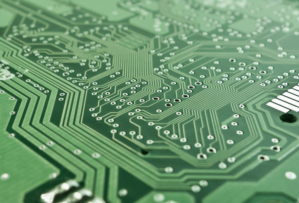
The wide bandgap semiconductor Gallium Nitride (GaN) has many advantageous properties, but it has been difficult to scale up production.
During such an invigorating period in the industry, silicon semiconductors have been in massive demand. And in short supply. It has not been the best time to consider switching to a new wafer material. Not that there ever will be a quiet moment in this sector.
Where it all beGaN
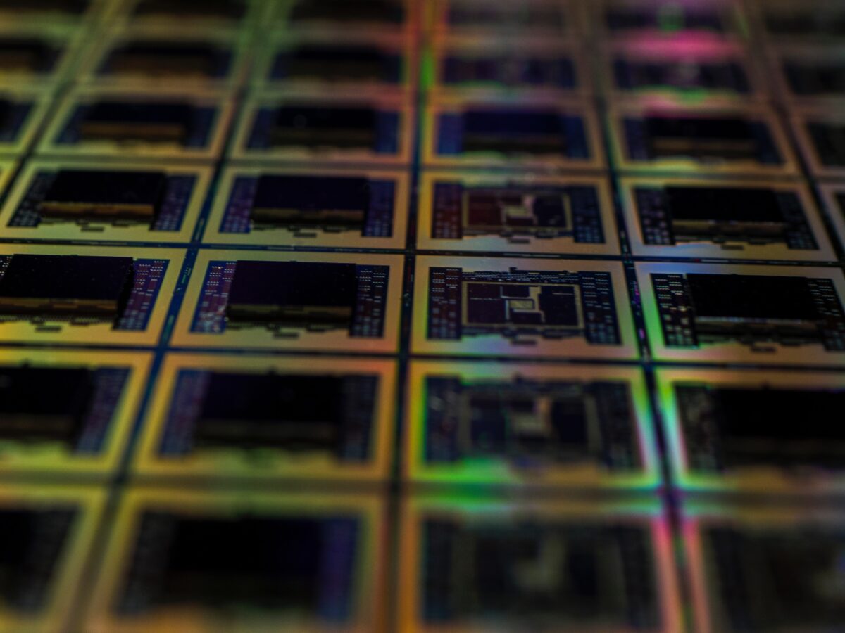
GaN has only really been in the picture since the mid-90s, when its top uses were military. Since then it has seen growth, with a revenue of $1 billion in 2020 according to Strategy Analytics. Silicon wafer revenue, in comparison, was $11.2 billion. GaN is still a small fry.
Despite GaN production being a much smaller endeavour currently, there are several companies currently manufacturing GaN devices. GaN is currently used for power electronic devices thanks to their high electron mobility and high breakdown voltages.
A survey was undertaken by Microwave Journal, wherein they contacted major GaN suppliers around the world. Of the 8 that responded, there were 36 variants available, with gate lengths ranging between 0.5ɥm to 40nm. The GaN variants included GaN-on-SiC, GaN on Si and GaN on diamond substrates.
The potential future of semiconductors
We’ve talked before about how GaN could be a future replacement for the aging silicon semiconductors. This would not only benefit consumers because of its fast performance, but would also benefit the environment.
The first and most obvious factor, is that with more efficient semiconductors less of them would be required. GaN requires less raw material and because of the reduced size there can be more units per wafer.
Aside from this, the actual manufacturing emissions for GaN are much lower. Gallium metal is a by-product of aluminium smelting, and nitrogen is readily available in the atmosphere. GaN, then, has a minimal carbon footprint and is easily sourced.
If GaN could be used globally, it could make a difference against climate change, more than silicon or silicon carbide. It is also non-toxic and includes no conflict materials. GaN power IC devices can also be manufactured using already-established CMOS processing equipment.
It’s not GaNna be easy…
So GaN could well be a great alternative for silicon in years to come, however the problem comes with up-scaling production and transitioning. Changing the semiconductor material would undoubtedly incur several design and logistical changes, and would cause disruptions and delays.
Some industry experts have suggested investing in mega-fabs to produce GaN-on-Si wafers for manufacturers. This would help even out the disparity between GaN and silicon stock, and encourage more manufacturers to produce GaN devices.
It’s estimated that the GaN-based power IC management market will grow by about 70% each year from 2020 to 2026. This is just one use of GaN, but demonstrates how profitable the material may be in the future.
Lantek has a huge range of stock which includes both brand new electronic components and obsolescent stock. Whatever you may need Lantek can provide it. Get in touch with us today to see what we can do for you! Contact us on sales@lantekcorp.com or call us on 1-973-579-8100
This blog is purely for entertainment and informational purposes, it is in no way instructional.