Categories
Electronic Components Technology

The Chips Act childcare clause

The Chips Act childcare clause

Semiconductor manufacturers will have to provide affordable childcare for their workers, according to a clause in the Chips Act.

New regulations will mean that companies are required to provide day-care facilities near to their manufacturing sites. They could also provide subsidies to workers so they can pay for childcare separately.

This clause only applies to companies applying for $150 million or more in funding, but other applicants are also advised to put these measures in place.

The NOFO

These measures were released in the First Notice of Funding Opportunity (NOFO) on February 28th. It covers not only childcare provisions, but other measures to improve support for the workforce and their community.

Secretary of the Commerce Department, Gina Raimondo, praised the inclusion of a childcare clause. She has said in the past that a lack of childcare provisions prevented people from returning to work post-pandemic.

According to Raimondo, manufacturers and unions need to work with the department towards some grand goals. She hopes they can hire and train another million women in construction in the next ten years. This, she said, will help meet demand not only in the chip industry but across other industries.

Other requirements

Other provisions in the first NOFO require applicants to show their understanding of the Chips Act’s objectives. They also have to demonstrate partnerships with local governments, a plan for workforce training and supply chain risk and intellectual property theft mitigation plans.

Both the NOFO and the original legislation in the Chips Act will bring any foreign investment under a microscope. While foreign companies can apply for certain manufacturing incentives, there are stipulations. This include ineligibility if the country is listed as a ‘foreign entity of concern’, or if the application is funded by one.

There will be two further NOFOs released further down the line. The second NOFO will be based around semiconductor materials and equipment, and the third will be for R&D facilities.

Act now

Despite all the changes to chip legislation in the US, Lantek is not going anywhere. We will continue to do the best for our customers and make sure all their electronic component needs are met. Whether you’re based at home or internationally, we will harness our global network to ensure you always have what you need. Call us today on 1-973-579-8100, or email us at sales@lantekcorp.com to change your supply chain for the better.

Categories
Technology

US solar industry stalled by goods restrictions

US solar industry stalled by goods restrictions

US solar panel installations are expected to decline by almost a quarter due to several restrictions being put in place. Among these, there is a new import ban on products from China’s Xinjiang region, and restrictions on products from companies found to be dodging tariffs.

Some companies were found to be avoiding tariffs by finishing their products in Southeast Asian countries. This led to a ban on importing products from these companies, which was later waived by Biden. Other companies, working in a controversial region of China, were also restricted by the US.

More than 1000 solar energy import shipments have stalled at US ports since new legislation came into effect in June.

The law

The legislation came in just months before the Inflation Reduction Act (IRA) was also signed into law. This Act encourages the use of clean energy technologies against the effects of climate change. Many domestic solar companies hope to benefit from the Act, which allocates almost $400 billion in funding for clean energy.

However, since the restrictions have been announced there’s expected to be delays until late 2023.

Currently, the largest markets for solar technology are utilities and other commercial customers. The residential market is expected to increase by 37%.

Although the restrictions will impede the growth of domestic solar project developers, there are certain reliefs. Only some of the solar panel manufacturers from China have been restricted, so other imports are still available.

Further developments

More recently, though, China has also suggested they would ban the export of its solar panel technology. China controls about 75% of the solar panel industry right now. Even with the current restrictions, this move could have a huge impact on the US.

More than anything, policy-makers and manufacturers in the US are concerned about the time it would take to catch up. The solar industry has been so reliant on Chinese suppliers over the years, it won’t be easy to wean off.

The Biden administration did put a 2-year waiver in place to delay some of the restrictions coming in, but this will not go all the way to avoid delays. Building a single factory to make a material like polysilicon would take a few years. Recreating the entire supply chain could take 4 times as long.

Choose reliability

Whether you’re looking for solar panel components or any other electronic parts, choose Lantek. We have a dedicated sales team on hand to find all of the components you want. Call us today on 1-973-579-8100 or email us at sales@lantekcorp.com. We’ll be waiting!

Categories
Electronic Components Supply Chain Technology

New US India semiconductor partnership

New US India semiconductor partnership

The US recently formed a partnership with India with an aim to cooperate in several industries, including semiconductor production. This is
hoped to be a very fruitful partnership, especially since the increase in restrictions between China and the US.

Recent changes

More companies have been investing in India in recent years, including Vedanta-Foxconn, PSMC and Micron Technology. Partly thanks to new government incentive schemes, companies are trying to move manufacturing into the country. More are expected to follow as India increases its funding for semiconductor manufacturing.

The Indian Government and related parties have announced several incentives for incoming companies. One of the largest was that there would be a 50% waiver on the cost of establishing a fab.  

The US and Indian Semiconductor Associations (SIA and IESA respectively) have also formed a taskforce to strengthen collaboration. The taskforce plans to assess the country’s readiness to sustain a semiconductor market and make recommendations to increase its presence in the
supply chain.

But it hasn’t been easy. Many incoming companies have mentioned difficulties with a lack of infrastructure, difficult regulations, and other struggles.

The competition

India could also potentially help in the sourcing of minerals for semiconductor production. Currently much of the world’s supply (72%)
comes from China, which could prove troublesome soon enough. 

However, India is apparently abundant in 49 critical and non-fuel minerals that are used in the industry according to a report by the Council on Energy, Environment and Water (CEEW) and the Ministry of Science and Technology.

Work away


Another potential benefit to the States is the new ‘friend-shoring’ location it has unlocked. While the Chips Act attempts to move much of the
process to domestic, this won’t be entirely achievable.

The high cost of labor and the lack of highly-skilled employees within the field will prove challenging. In a collaboration with India, however, it would provide a manufacturing location with manageable labor costs. It could also pave the way for highly-skilled professionals from India
to work in the US.

There are hopes that this collaboration is the next big milestone for the countries since the 2016 nuclear power agreement.

A different kind of partnership

We have a steadfast relationship with all of our customers, thanks to the trust and reliability we are known for. Lantek Corporation can fulfil
all your electronic part needs, all you need to do is contact us. We’re available at sales@lantekcorp.com or call us on 1-973-579-8100.

Categories
Technology

What alternatives to WiFi are available?

What alternatives to WiFi are available?

WiFi has been an integral part of our life since the 90s when it first came into being. Originally created for wireless connections in cashier systems under the name WaveLAN, the trademarked WiFi name came into existence just before the turn of the century and hasn’t looked back since.

Alongside WiFi, cellular internet was also thriving, giving people the power to connect to a network through a phone signal. The current rollout of 5G shows that this method of connecting to the internet is also still very popular and getting more advanced by the year.

But since the conception of these two types of communications, several new methods have also been designed, and may be contenders to replace them in future.

How does WiFi work?

WiFi stands for Wireless Fidelity and uses radio waves to transmit signals between devices. The frequency is in the Gigahertz range, as opposed from Kilohertz and Megahertz for AM and FM radio respectively. This is why every iteration of cellular internet has a ‘G’ after it, because the frequency range for WiFi is between 2.4GHz and 5GHz.

But, as with all things, there are limitations to WiFi’s capabilities. Many current devices can’t yet use 5G as they weren’t built to support it, and 2.4G is now so congested it is almost always unusable too.

LiFi

This WiFi alternative, known as Light Fidelity, was first announced in 2011 during a TED Global Talk by Professor Harald Haas where he demonstrated it for the first time. The system uses light instead of radio waves, so lightbulbs can create a wireless type of network.

Despite the term being first coined by Haas, CSO of PureLiFi, several companies have since introduced products with strikingly similar names that also use light. This type of communication is called Optical Wireless Communications (OWC), which encompasses communications using infrared, ultraviolet and visible light.

Satellite WiFi

Starlink is just one example out of the category of satellite WiFi. The SpaceX subdivision uses a network of private satellites positioned across the globe to provide internet access. Currently the company has around 2,000 working satellites orbiting the planet.

Although this is already an established form of internet access, especially in rural areas, the investment in developing this technology and its versatility makes it a contender for the monopoly on WiFi in the future.

Mesh Networking

Mesh networks are often used as an extension to a regular WiFi home connection. The short-range network uses two modulation techniques, Binary and Quadrature Phase-shift Keying (BPSK and QPSK). This makes the mesh network devices act like high-speed Ultra-wideband ones.

The system works on the principle that you install nodes, like mini satellites, throughout your house. The nodes all act as stepping stones, which means the WiFi signal at any point in your house will be much stronger than if you only had one central router.

The fibre-optic future

With the recent advent of 5G and the increasing availability of faster WiFi thanks to tech like fibre optic broadband, it’s unlikely it will go out of fashion very soon. But it’s always nice to have a bit of choice, isn’t it?

One huge benefit that comes with the internet is being able to find electronics component suppliers at high speed. Whether you’re on satellite WiFi, cellular, or LiFi, contact lantek today at sales@lantekcorp.com to see how we can help you.

Categories
Technology

What is the Internet of Things?

What is the Internet of Things?

EveryThing

In terms of IoT, a ‘Thing’ is anything that can transfer data over a network and can have its own IP address. They are most often ‘smart’ devices, that use processors or sensors to accumulate and send data.

These devices have little-to-no need for human interaction, except in cases where the smart device is controlled by a remote control or something similar. Due to the low cost of electronic components and wireless networks being readily available, it’s possible for most things to become, well, Things.

Technically, larger items like computers, aeroplanes, and even phones, cannot be considered IoT devices, but normally contain a huge amount of the smart devices within them. Smaller devices, however, like wearable devices, smart meters and smart lightbulbs can all be counted as IoT items.

There are already more connected IoT devices than there are people in the world, and as more Things are produced this progress shows no sign of slowing.

Applications of IoT

The automation and smart learning of IoT devices has endless uses and can be implemented in many industries. The medical industry can use IoT to remotely monitor patients using smart devices that can track blood pressure, heart rate and glucose levels, and can check if patients are sticking to treatment plans or physiotherapy routines.

Smart farming has garnered attention in recent years for its possibly life-saving applications. The use of IoT devices in the agricultural industry can enable the monitoring of moisture levels, fertiliser quantities and soil analysis. Not only would these functions lower the labour costs for farmers substantially but could also be implemented in countries where there is a desperate need for agriculture.

The industrial and automotive industries also stand to benefit from the development of IoT. Road safety can be improved with fast data transfer of vehicle health, as well as location. Maintenance could be performed before issues begin to affect driving if data is collected and, alongside the implementation of AI, smart vehicles and autonomous cars could be able to drive, brake and park without human error.

What’s next?

The scope of possibilities for IoT will only grow as technology and electronics become more and more accessible. An even greater number of devices will become ‘smart’ and alongside the implementation of AI, we will likely have the opportunity to make our lives fully automated. We already have smart toothbrushes and smart lightbulbs, what more could be possible in the future?

To make it sustainable and cost-effective, greater measures in security and device standardisation need to be implemented to reduce the risk of hacking. The UK government released guidelines in 2018 on how to keep your IoT devices secure, and a further bill to improve cyber security entered into law in 2021.

If you’re looking for chips, processors, sensors, or any other electronic component, get in touch with Lantek today. We are specialists in day-to-day and obsolete components and can supply you where other stockists cannot.

Contact Cyclops today at sales@lantekcorp.com. Or use the rapid enquiry form on our website to get fast results.

Categories
Electronic Components Technology

New construction of the smallest microchips using graphene nano-origami

New construction of the smallest microchips using graphene nano-origami

Material science and clever engineering have cut the space between components on microchips to nanometres. This has led to significant performance benefits because more components can fit on the chip.

However, there is a limit to how small things can go with the current chip design. 7nm is as small as chips will go from here based on existing technology. Why? Because 7nm is the gap between components on a chip. This space is tiny. Going smaller isn’t feasible because we’re working with spaces that are too small.

It’s also incredibly expensive. Prototyping a 7nm chip costs around £80 million and there are only a handful of companies that can do it.

Graphene ‘nano-origami’ to the rescue

Graphene is a nanomaterial one atom thick. It has been talked about as a revolutionary material for over a decade and now experimental researchers have used it to develop the world’s tiniest microchips using a form of ‘nano-origami’.

The world’s tiniest microchips are 100 times smaller than silicon chips and thousands of times faster. The way they work is instead of having transistors on them, the graphene has kinks in the structure and these kinks act as the transistors.

On this breakthrough, Prof Alan Dalton in the School of Mathematical and Physics Sciences at the University of Sussex, said:

“We’re mechanically creating kinks in a layer of graphene. It’s a bit like nano-origami. Using these nanomaterials will make our computer chips smaller and faster.

It is absolutely critical that this happens as computer manufacturers are now at the limit of what they can do with traditional semiconducting technology. Ultimately, this will make our computers and phones thousands of times faster in the future.”

Is graphene the future of microchips?

Researchers are calling this breakthrough nano-origami technology “straintronics”. It uses nanomaterials as opposed to electronics, eliminating the need for electronic components on the chip. This makes the chips 100 times smaller.

Another benefit to graphene microchips is speed. Graphene conducts electricity 250 times faster than silicon. In fact, it conducts electricity faster than any known substance. It truly is a ‘space-age’ nanomaterial for today.

Instead of building microchips with foreign materials like transistors, researchers have shown another way of doing things. By creating kinks in graphene, structures can be made that replace electronic components including transistors and logic gates.

Another benefit to graphene nano-origami is sustainability. No additional materials are added during the manufacturing process. Production also takes place at room temperature as opposed to high temperature with silicon chips.

The truth is that silicon microchips cannot feasibly go below 7nm. The next step in performance evolution with silicon chips will come from heat management and power density. Graphene is smaller, faster and just as capable. The next step is for manufacturers to develop the technology and take it to market.

Overall, while the immediate future is silicon, we are in no doubt that graphene is the future of microchips. It has too many performance advantages to ignore.   

Categories
Electronic Components Technology

Active and passive components to see strong 5G-driven demand

5G-driven demand coming for Active & Passive Components

As the international rollout of 5G picks up pace, active and passive component demand is increasing at a rate of knots.

The buildout of 5G infrastructure requires significant investment in active and passive components for a wide range of different devices.

Examples include active antennas with integrated RF radio designs, small cell power base stations, C-RAN architecture and semiconductors.

One of the challenges faced with the 5G rollout this year has been COVID-19, which had immediate effects on global supply in demand. Some of the side effects included increased costs, a slowdown in logistics, and a squeeze on demand.

While these challenges were significant in early 2020 and are likely to remain for some time, the macroeconomics are unlikely to persist in their worst form.

Right now, the manufacturing sector in most countries is bouncing back fast and many manufacturers are having their best ever quarter.

A good example is Taiwan Semiconductor, who are the largest semiconductor foundry in the world. Then you have smaller but vital players like MaxLinear, who make wireless, PON, DSL, and terrestrial products for high-speed internet.

How 5G is driving demand for active and passive components

You can think of 5G as a tide that is going to raise all ships, and active and passive components manufacturers are the ships that will benefit from it most because they will make the components that build out the 5G infrastructure.

It’s easy to see why this is the case with a short list of active and passive components. Let’s start with examples of passive components first:

  • Resistors
  • Inductors
  • Capacitors
  • Transformers

Now let’s list a few active components:

  • Generators
  • Transistors
  • Diodes
  • Inductors / coils

Now let’s look at a few of the components that will build out 5G:

  • Semiconductors
  • Antennas
  • Radio towers
  • RF receivers
  • Fibreoptic cable

Looking at these lists, it’s easy to see why 5G is driving such strong demand for active and passive components.

Can the components sector keep pace?

There are so many different manufacturers of electronic components that it is unlikely that the rollout of 5G will trouble the manufacturing sector.

However, local supply problems may exist for some enterprises. For example, a supplier of radio frequency devices in China may have to temporary shut production at a factory due to a fire or a health hazard. This would affect supply.

The best way for those involved in the rollout of 5G to safeguard their supply of active and passive components is to use an electronic component distributor. Electronic component distributor specialise in the procurement and delivery of electronic components and parts, so they can ensure you always have what you need.

A faster, more connected future awaits

5G will revolutionise our use of the internet in more ways than one, but the buildout is going to take time. Demand for active and passive components is at an all-time high, and competition is increasing for the best components. Having a component distributor on your side is a good way to ensure you can meet the challenge.

Click Here to use our fast component search and enquire with us today!

Categories
Electronic Components Technology

What does the future hold for the electronic component industry?

What does the future hold for the electronic component industry?

The future of the electronic component industry looks very healthy indeed thanks to tailwinds from 5G, robotics and automation, artificial intelligence, edge computing and several other emerging technologies.

A few of the companies destined to benefit from the advancement of these technologies include Infineon Technologies, STMicroelectronics, Würth Elektronik, Eaton Corp, Micron, MaxLinear, Hitachi and Qualcomm. There are hundreds more who are operating foundries and factories at maximum capacity to meet demand already.

Key to meeting the demand is an increase in manufacturing capability, which many companies will have to build through capital expenditure. We are already seeing an increase in investment from many of the aforementioned companies.

As for electronic component distributors, the phrase “a rising tide raises all ships” is a perfect expression. Component distributors like us will see an increase in demand in the future as our world becomes more technology-focussed.

These are the technologies that we see fuelling electronic component growth in the near future (we already mentioned a few in our opening paragraph):

  • 5G
  • Wi-Fi 6
  • Big data
  • Edge computing
  • AI
  • Robotics
  • Biotechnology
  • Batteries and power
  • Displays
  • Semiconductors and GPUs
  • Automated driving
  • Consumer electronics: VR, AR, smartphones, tablets

Every infrastructure, and every product, will need a unique set of electronic components in its design. Factories and foundries will make the components, and electric component distributors will help manufacturers source them.

Meeting the uptick in demand

There’s one certainty in the electronics industry: demand on components increases as technologies become more complex. We see this with semiconductors, which are getting smaller (2nm), with 5G, which requires more components than 4G, and in robotics, which require powerful Lidar guidance systems.

To meet this uptick in demand, there are companies that specialise in making specific components and machines.

For example, Axcelis Technologies, headquartered in Beverly, Massachusetts, makes ion implant equipment vital to semiconductor fabrication. Then we have Micron, who recently announced high-density 3D NAND flash memory.

The innovation and investment in new technologies from leading companies is a clear sign that the electronic component industry is not just healthy, but thriving, despite the disruption caused by COVID-19.

The role of electronic component distributors

Our place in all this as an electronic component distributor is to help our customers (who include OEMs, foundries, factories and assemblers) to source the components they need to operate their business.

We are crucial to our customers because we are a global distributor. We enable industry players to buy electronic components with confidence at competitive prices, and our links in the industry allow our customers to gain a competitive edge.

As demand has increased for electronic components, competition has intensified, and it really isn’t uncommon for companies to have to bid for components. This is the result of a market that doesn’t produce enough components for certain applications. We exist to help all companies source the components they need.

With us, you get a fast response to your enquiries and reliable on time delivery. There’s no better partner to have on your side.

Click Here and visit our site today to use our fast component search tool and enquire with us today!


Categories
Electronic Components Technology Transistors

The multimodal transistor (MMT) is a new design philosophy for electronics

Researchers from the University of Surrey and University of Rennes have developed a technology called the multimodal transistor (MMT), which could revolutionise electronics by simplifying circuits and increasing design freedom.

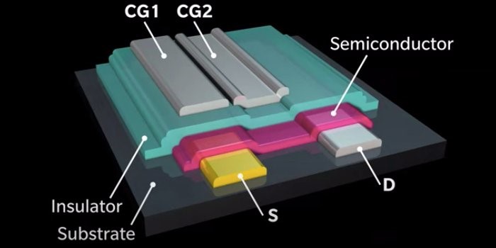
The multimodal transistor is a thin-film transistor that performs the same job as more complex circuits. The MMT sandwiches metals, insulators and semiconductors together in a package that’s considerably thinner than a normal circuit.

However, the key breakthrough with the MMT is its immunity to parasitic effects (unwanted oscillations). The MMT allows consistent, repeatable signals, increasing a transistor’s performance. This is necessary for precision circuits to function as intended and is especially useful for next-gen tech like AI and robotics.

How it works

In the image below, we can see the design of the MMT. CG1 provides the means to control the quantity of charge, while CG2 is the channel control gate. CG1 controls the current level and CG2 controls the on/off state.

This is a massive shift in transistor design because it enables far greater engineering freedom. It is a simple and elegant design, yet it is so useful. It has numerous applications in analogue computation and hardware learning.

Digital-to-analogue conversion

MOSFET transistors are one of the building blocks of modern electronics, but they are non-linear and inefficient.

In a conventional circuit, gate electrodes are used to control a transistor’s ability to pass current. The MMT works differently. Instead of using gate electrodes, it controls on/off switching independently from the amount of current that passes through. This allows the MMT to operate at a higher speed with a linear dependence between input and output. This is useful for digital-to-analogue conversion.

The breakthrough in all its glory

The MMT transforms the humble transistor into a linear device that delivers a linear dependence between input and output. It separates charge injection from conduction, a new design that achieves independent current on/off switching.

There is a profound increase in switching speed as a result of this technology, enabling engineers to develop faster electronics. Researchers estimate that the switching speed is as much as 10 times faster. Also, fewer transistors are needed, increasing the yield rate and reducing the cost to manufacture the circuit.  

Just how revolutionary the MMT will be remains to be seen. After all, this is a technology without commercialisation. It could find its way into the electronics we use on a daily basis, like our phones. The potential is for the MMT to be printable, allowing for mass production and integration into billions of electrical devices.

With devices getting smarter and digital transformation advancing at a rapid rate, the electronics industry is booming. Semiconductor foundries are at peek capacity and more electrical devices are being sold than ever. The MMT is a unique solution to a problem, and it could make manufacturing electronics cheaper.   

With this, comes a great opportunity for the MMT to replace MOSFET transistors. We can think of few other design philosophies with such wicked potential.

Categories
Electronic Components Technology

How “Chiplets” May Help the Future of Semiconductor Technology

How 'Chiplets' may help the future of Semiconductor Technology

The global demand for semiconductors is accelerating faster than a speeding bullet, with integrated device manufacturers, systems companies, and foundries like Taiwan Semiconductor Manufacturing Company making a killing.

This accelerating demand is largely fuelled by the rollout of 5G infrastructure and the increasingly connected devices we use on a daily basis. From semi-autonomous driving aids to the connected home, semiconductors power our digital lives. They are the brains of every smart electronics operation.

In the semiconductor industry, advancements come fast. Some companies have been painfully slow to react to change. Intel is a good example – they have fluffed the development of their 7nm chips and are stuck at 12nm, while AMD already has 7nm chips and is on course to deliver a 5nm chip. Nvidia is even further ahead.  

Chiplets

Chiplets are a proven (but niche) way for semiconductor developers to make semiconductors more efficient and easier to produce.

As semiconductors get more advanced, they get smaller. At a sub 10nm scale, foundries have to be spotlessly clean. This brings with it manufacturing complexities. Also, the smaller transistors get, the more likely they are to fail.

You can increase the yield of dies with small transistors by reducing overall size. But as you reduce the size of the die, you have less space for the transistors.

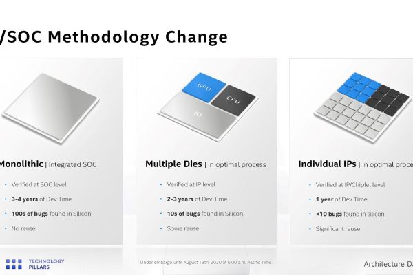
So, one solution is Chiplets. Chiplets are smaller functional dies that integrate multiple chiplets into a single semiconductor. By giving functions their own circuits (sub-circuits) we can remove design complexity and focus on efficiency.

Maximising yield reduces cost

Using chiplets maximises the yield of dies and reduces design complexity, which in turn reduces manufacturing cost. To give you an idea of by how much, AMD says chiplet designs can cut costs by more than half. 50%! That’s an astonishing saving and worth the effort if it also means keeping up with technological change.

(For what it’s worth, AMD uses chiplet design in its Zen 2 and Ryzen chips. The idea being that taking smaller dies and putting them together improves yield).

Intel is also a fan of chiplet design, and they have a vision for advancing it further, where instead of multiple dies, each IP has its own building block. This creates a more modular and flexible configuration. Here’s an illustration:

chiplet internal image

This is an exciting technology because the chiplets with IP/SOC are considerably smaller than the chiplets used in multiple dies. The benefit of this is you can configure the chiplets in more ways and maintain a common architecture.

Chiplets – the future, or not?

Chiplet design is already being used by AMD, and Nvidia has said they will go chiplet when it’s economically viable to do so. This means two of the three biggest CPU and GPU companies on the planet are on the chiplet train. As for Intel, they are too – but it looks like they will go their own way to build the chiplet model they want.

Clearly, chiplets are here to stay. Scaling chips with monolithic dies will always be a thing, but it gets expensive with advanced nodes. Chiplets are necessary to break up the cost and deliver the massive number of chips our connected world needs.