The global demand for semiconductors is accelerating faster than a speeding bullet, with integrated device manufacturers, systems companies, and foundries like Taiwan Semiconductor Manufacturing Company making a killing.
This accelerating demand is largely fuelled by the rollout of 5G infrastructure and the increasingly connected devices we use on a daily basis. From semi-autonomous driving aids to the connected home, semiconductors power our digital lives. They are the brains of every smart electronics operation.
In the semiconductor industry, advancements come fast. Some companies have been painfully slow to react to change. Intel is a good example – they have fluffed the development of their 7nm chips and are stuck at 12nm, while AMD already has 7nm chips and is on course to deliver a 5nm chip. Nvidia is even further ahead.
Chiplets
Chiplets are a proven (but niche) way for semiconductor developers to make semiconductors more efficient and easier to produce.
As semiconductors get more advanced, they get smaller. At a sub 10nm scale, foundries have to be spotlessly clean. This brings with it manufacturing complexities. Also, the smaller transistors get, the more likely they are to fail.
You can increase the yield of dies with small transistors by reducing overall size. But as you reduce the size of the die, you have less space for the transistors.
So, one solution is Chiplets. Chiplets are smaller functional dies that integrate multiple chiplets into a single semiconductor. By giving functions their own circuits (sub-circuits) we can remove design complexity and focus on efficiency.
Maximising yield reduces cost
Using chiplets maximises the yield of dies and reduces design complexity, which in turn reduces manufacturing cost. To give you an idea of by how much, AMD says chiplet designs can cut costs by more than half. 50%! That’s an astonishing saving and worth the effort if it also means keeping up with technological change.
(For what it’s worth, AMD uses chiplet design in its Zen 2 and Ryzen chips. The idea being that taking smaller dies and putting them together improves yield).
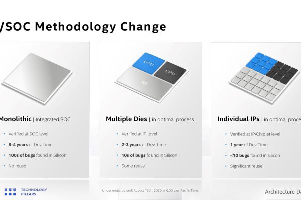
Intel is also a fan of chiplet design, and they have a vision for advancing it further, where instead of multiple dies, each IP has its own building block. This creates a more modular and flexible configuration. Here’s an illustration:

This is an exciting technology because the chiplets with IP/SOC are considerably smaller than the chiplets used in multiple dies. The benefit of this is you can configure the chiplets in more ways and maintain a common architecture.
Chiplets – the future, or not?
Chiplet design is already being used by AMD, and Nvidia has said they will go chiplet when it’s economically viable to do so. This means two of the three biggest CPU and GPU companies on the planet are on the chiplet train. As for Intel, they are too – but it looks like they will go their own way to build the chiplet model they want.
Clearly, chiplets are here to stay. Scaling chips with monolithic dies will always be a thing, but it gets expensive with advanced nodes. Chiplets are necessary to break up the cost and deliver the massive number of chips our connected world needs.
| Cookie | Duration | Description |
|---|---|---|
| cookielawinfo-checkbox-analytics | 11 months | This cookie is set by GDPR Cookie Consent plugin. The cookie is used to store the user consent for the cookies in the category "Analytics". |
| cookielawinfo-checkbox-functional | 11 months | The cookie is set by GDPR cookie consent to record the user consent for the cookies in the category "Functional". |
| cookielawinfo-checkbox-necessary | 11 months | This cookie is set by GDPR Cookie Consent plugin. The cookies is used to store the user consent for the cookies in the category "Necessary". |
| cookielawinfo-checkbox-others | 11 months | This cookie is set by GDPR Cookie Consent plugin. The cookie is used to store the user consent for the cookies in the category "Other. |
| cookielawinfo-checkbox-performance | 11 months | This cookie is set by GDPR Cookie Consent plugin. The cookie is used to store the user consent for the cookies in the category "Performance". |
| viewed_cookie_policy | 11 months | The cookie is set by the GDPR Cookie Consent plugin and is used to store whether or not user has consented to the use of cookies. It does not store any personal data. |
This website uses cookies to improve your experience. We'll assume you're ok with this, but you can opt-out if you wish. Read More
