Categories
Electronic Components

Improvements to smart materials in the works

Improvements to smart materials in the works

A team of scientists and engineers has developed a new way of producing thin film perovskite semiconductors.

This ‘smart material’ can adapt depending on stimuli like light, magnetic fields or electric fields.

This could lead to the material being combined with other nano-scale materials to produce sensors, smart textiles and flexible electronics.

Thin films are usually made via epitaxy: atoms are placed on a substrate one layer at a time.

However, with this method the films stay attached to the host substrate and are less easily utilised. If it can be separated from the substrate it is much more useful.

The team, based at the University of Minnesota, has found a way to create a strontium titanate membrane without several of the usual freestanding membrane issues.

Making freestanding ‘smart’ oxide material membranes comes with certain challenges. Unlike 2D substances like graphene, smart oxide materials are bonded in 3 dimensions.

The method

One way to make them is using remote epitaxy. Graphene is used as an intermediary between the substrate and the membrane. This allows the thin film material to be peeled off the substrate. One issue with this is when using the technique with metal oxides the graphene becomes oxidised and ruins the sample.

A new technique pioneered by the University of Minnesota is hybrid molecular beam epitaxy. This stops the oxidation process by using titanium that is already bonded to oxygen. The team has also been able to introduce automatic stoichiometric control, which no one else has been able to do.

The hope is in future to combine these thin film membranes to create more advanced smart materials. There are certain products already using thin films like gallium-oxide. Other alternatives to thin film include carbon nanotubes, which can be used in layers of only 0.06nm thickness.

A ‘smart’ choice

Lantek can provide a huge range of specialist, day-to-day, and hard to find electronic components. We work with our customers to make sure we find what they need and deliver in the quickest time possible.

Contact Lantek for all your electronic component needs. Call us at 1-973-579-8100 or email us at sales@lantekcorp.com

Categories
component shortage Covid-19 Electronic Components Supply Chain

Lantek 2022- a year in review

Lantek 2022- a year in review

As 2022 comes to an end, we at Lantek are reflecting on the many ups and downs of the year and the great things that will be happening in 2023. 

This year was yet another year of challenges for finding product and then the even bigger challenge to find stock at pricing that customers can afford. Lantek was able to work with many companies this year to help avoid lines down situations. The years of experience from all of our staff
played a major role in that.

Electronica

This past November we were able to meet up with long time and even some new customers at Electronica in Munich. Some conversations were
had about the market and where everyone sees it going but more importantly, it was a chance to just sit and talk face to face with people we haven’t seen since 2018!

Frank Cervino, our GM, said this: “After so many years, catching up with customers and suppliers during these uncertain market
conditions was very beneficial. It was also a pleasure to spend time with the Cyclops Group and be present on the stand.”

Christmas

As our year ends on December 22, we will be having a Christmas lunch brought in for us all to enjoy.

In January, Lantek will be marking its 29th year in business and what a way to celebrate but with our new office and warehouse
space!

We are hoping to be able to start moving product by mid-February.

We will take volunteers to help with that! (If any of you have ever been to NJ in the winter, you will appreciate the challenge this will be)

See you next year!

In closing we would like to wish all of you a very happy holiday season and may your 2023 be a prosperous and positive one!

We will be back in the office on January 3, 2023 for any and all of your electronic component needs. Please contact us at 973.579.8100 or at sales@lantekcorp.com.

Categories
Electronic Components

Should we be investing in GaN fabs?

Should we be investing in GaN fabs?

The wide bandgap semiconductor Gallium Nitride (GaN) has many advantageous properties, but it has been difficult to scale up production.  

During such an invigorating period in the industry, silicon semiconductors have been in massive demand. And in short supply. It has not been the best time to consider switching to a new wafer material. Not that there ever will be a quiet moment in this sector.

Where it all beGaN

GaN has only really been in the picture since the mid-90s, when its top uses were military. Since then it has seen growth, with a revenue of $1 billion in 2020 according to Strategy Analytics. Silicon wafer revenue, in comparison, was $11.2 billion. GaN is still a small fry.

Despite GaN production being a much smaller endeavour currently, there are several companies currently manufacturing GaN devices. GaN is currently used for power electronic devices thanks to their high electron mobility and high breakdown voltages.

A survey was undertaken by Microwave Journal, wherein they contacted major GaN suppliers around the world. Of the 8 that responded, there were 36 variants available, with gate lengths ranging between 0.5ɥm to 40nm. The GaN variants included GaN-on-SiC, GaN on Si and GaN on diamond substrates.

The potential future of semiconductors

We’ve talked before about how GaN could be a future replacement for the aging silicon semiconductors. This would not only benefit consumers because of its fast performance, but would also benefit the environment.

The first and most obvious factor, is that with more efficient semiconductors less of them would be required. GaN requires less raw material and because of the reduced size there can be more units per wafer.

Aside from this, the actual manufacturing emissions for GaN are much lower. Gallium metal is a by-product of aluminium smelting, and nitrogen is readily available in the atmosphere. GaN, then, has a minimal carbon footprint and is easily sourced.

If GaN could be used globally, it could make a difference against climate change, more than silicon or silicon carbide. It is also non-toxic and includes no conflict materials. GaN power IC devices can also be manufactured using already-established CMOS processing equipment.

It’s not GaNna be easy…

So GaN could well be a great alternative for silicon in years to come, however the problem comes with up-scaling production and transitioning. Changing the semiconductor material would undoubtedly incur several design and logistical changes, and would cause disruptions and delays.

Some industry experts have suggested investing in mega-fabs to produce GaN-on-Si wafers for manufacturers. This would help even out the disparity between GaN and silicon stock, and encourage more manufacturers to produce GaN devices.

It’s estimated that the GaN-based power IC management market will grow by about 70% each year from 2020 to 2026. This is just one use of GaN, but demonstrates how profitable the material may be in the future.

Lantek has a huge range of stock which includes both brand new electronic components and obsolescent stock. Whatever you may need Lantek can provide it. Get in touch with us today to see what we can do for you! Contact us on sales@lantekcorp.com or call us on 1-973-579-8100

This blog is purely for entertainment and informational purposes, it is in no way instructional.

Categories
Electronic Components

Electronics to measure climate change

Electronics to measure climate change

Semiconductors are being used to track and combat the effects of climate change. Their use could help scientists better understand the impact and process global warming has on the planet.

Climate change and global warming are topics that are often discussed in modern society, both by governments and individuals alike. There are certain industries that are thought to be larger contributors to the current situation. However, the electronics industry may be able to help rather than hinder the battle against climate change.

Accelerometers

These electronic components have been used to measure the effects of climate change through trees.

Accelerometers measure the vibration or acceleration of motion of a structure. Inside is a piezoelectric material, which makes an electrical charge proportional to the force caused by the motion.

The electronic device can be used for a variety of things, from spaceships to smartphones. But recently, researchers have been tying them to trees.

These so-called ‘tree fitbits’ can track the timing of tree activities like blooming or the leaves changing. Two ash trees in East Boulder were fitted with high-resolution accelerometers which tracked how they responded to the changing seasons.

The hope is that in the future tree phenology (the study of periodic events in biological life cycles) can be studied in relation to climate change. The accelerometers measured the amount that the trees swayed and the high frequency vibrations of the tree itself. This helps scientists track the phases of the tree (phenophases) as the seasons progress.

The data means that the start and end of each season for the tree, for example flowering in spring, can be measured and compared to data from previous years. The differences can be indicative of climate change and could be used as a warning sign.

Sensors

Miniscule sensors inspired by dandelion seeds could be scattered to track climate change indicators as well. The sensors were produced by a team from the University of Washington in Seattle. The electronic devices are made from polyimide films, and were manufactured using a laser-powered tool. Throughout its structure there are tiny holes, which aids it in floating like a dandelion seed.

The benefit of these tiny sensors means researchers can reach dangerous places without putting themselves at risk. Tracking temperature, humidity and other environmental signals across a large area would be beneficial to climate change research.

On board there are tiny solar panels and a capacitor that can store energy overnight when conditions are not optimal.

Indicators of change?

The future of the planet is not set in stone, and electronic devices can make a difference. Both in prediction and prevention, electronics are aiding us in our efforts. Lantek can provide electronic components for you to make your own change. Trust Lantek to supply you, contact us on sales@lantekcorp.com or 1-973-579-8100

This blog is purely for entertainment and informational purposes, it is in no way instructional.

Categories
Electronic Components

Thermal management of semiconductors

Thermal management of semiconductors

Too hot to handle

Every electronic device or circuit will create heat when in use, and it’s important to manage this. If the thermal output isn’t carefully controlled it can end up damaging, or even destroying the circuit.

This is especially an issue in the area of power electronics, where circuits reaching high temperatures are inevitable.

Passive thermal dissipation can only do so much. Devices called heat sinks can be used in circuits to safely and efficiently dissipate the heat created. Fans or air and water-cooling devices can be used also.

Feelin’ hot, hot, hot!

Using thermistors can help reliably track the temperature limits of components. When used correctly, they can also trigger a cooling device at a designated temperature.

When it comes to choosing a thermistor, there is the choice between negative temperature coefficient (NTC) thermistors, and positive temperature coefficient (PTC) thermistors. PTCs are the most suitable, as their resistance will increase as the temperature does.

Thermistors can be connected in a series and can monitor several potential hotspots simultaneously. If a specified temperature is reached or exceeded, the circuit will switch into a high ohmic state.

I got the power!

Power electronics can suffer from mechanical damage and different components can have different coefficients of thermal expansion (CTE). If components like these are stacked and expand at different rates, the solder joints can get damaged.

After enough temperature changes, caused by thermal cycling, degradation will start to be visible.

If there are only short bursts of power applied, there will be more thermal damage in the wiring. The wire will expand and contract with the temperature, and since both ends of the wire are fixed in place this will eventually cause them to detach.

The heat is on

So we’ve established that temperature changes can cause some pretty severe damage, but how do we stop them? Well, you can’t really, but you can use components like heat sinks to dissipate the heat more efficiently.

Heat sinks work by effectively taking the heat away from critical components and spreading it across a larger surface area. They usually contain lots of strips of metal, called fins, which help to distribute heat. Some even utilise a fan or cooling fluid to cool the components at a quicker speed.

The disadvantage to using heat sinks is the amount of space they need. If you are trying to keep a circuit small, adding a heat sink will compromise this. To reduce the risk of this as much as possible,  identify the temperature limits of devices and choose the size of heat sink accordingly.

Most designers should provide the temperature limits of devices, so hopefully matching them to a heat sink will be easy.

Hot ‘n’ cold

When putting together a circuit or device, the temperature limits should be identified, and measures put in place to avoid unnecessary damage.

Heat sinks may not be the best choice for everyone, so make sure to examine your options carefully. There are also options like fan or liquid-based cooling systems.

Cyclops Electronics can supply both electronic components and the heat sinks to protect them. If you’re looking for everyday or obsolete components, contact Lantek today and see what we can do for you.

Categories
Electronic Components

Electronic Components of a hearing aid

Electronic Components of a hearing aid

Hearing aids are an essential device that can help those with hearing loss to experience sound. The gadget comes in an analogue or digital format, with both using electronic components to amplify sound for the user.

Main components

Both types of hearing aid, analogue and digital, contain semiconductors for the conversion of sound waves to a different medium, and then back to amplified sound waves.

The main components of a hearing aid are the battery, microphone, amplifier, receiver, and digital signal processor or mini-chip.

The battery, unsurprisingly, is the power source of the device. Depending on the type of hearing aid it can be a disposable one or a rechargeable one.

The microphone can be directional, which means it can only pick up sound from a certain direction, which is in front of the hearing aid user. The alternative, omnidirectional microphones, can detect sound coming from all angles.

The amplifier receives signals from the microphone and amplifies it to different levels depending on the user’s hearing.

The receiver gets signals from the amplifier and converts them back into sound signals.

The digital signal processor, also called a mini-chip, is what’s responsible for all of the processes within the hearing aid. The heart of your hearing, if you will.

Chip shortages

As with all industries, hearing aids were affected by the chip shortages caused by the pandemic and increased demand for chips.

US manufacturers were also negatively impacted by Storm Ida in 2021, and other manufacturers globally reported that orders would take longer to fulfil than in previous years.

However, despite the obstacles the hearing aid industry faced thanks to covid, it has done a remarkable job of recovering compared to some industries, which are still struggling to meet demand even now.

Digital hearing aid advantages

As technology has improved over the years, traditional analogue hearing aids have slowly been replaced by digital versions. Analogue devices would convert the sound waves into electrical signals,  that would then be amplified and transmitted to the user. This type of hearing aid, while great for its time, was not the most authentic hearing experience for its users.

The newer digital hearing aid instead converts the signals into numerical codes before amplifying them to different levels and to different pitches depending on the information attached to the numerical signals.

Digital aids can be adjusted more closely to a user’s needs, too, because there is more flexibility within the components within. They often have Bluetooth capabilities too, being able to connect to phones and TVs. There will, however, be an additional cost that comes with the increased complexity and range of abilities.

Categories
Electronic Components

What are GaN and SiC?

What are GaN and SiC?

Silicon will eventually go out of fashion, and companies are currently heavily investing in finding its protégé. Gallium Nitride (GaN) and Silicon Carbide (SiC) are two semiconductors that are marked as being possible replacements.

Compound semiconductors

Both materials contain more than one element, so they are given the name compound semiconductors. They are also both wide bandgap semiconductors, which means they are more durable and capable of higher performance than their predecessor Silicon (Si).

Could they replace Silicon?

SiC and GaN both have some properties that are superior to Si, and they’re more durable when it comes to higher voltages.

The bandgap of GaN is 3.2eV and SiC has a bandgap of 3.4eV, compared to Si which has a bandgap of only 1.1eV. This gives the two compounds an advantage but would be a downside when it comes to lower voltages.

Again, both GaN and SiC have a greater breakdown field strength than the current semiconductor staple, ten times better than Si. Electron mobility of the two materials, however, is drastically different from each other and from Silicon.

Main advantages of GaN

GaN can be grown by spraying a gaseous raw material onto a substrate, and one such substrate is silicon. This bypasses the need for any specialist manufacturing equipment being produced as the technology is already in place to produce Si.

The electron mobility of GaN is higher than both SiC and Si and can be manufactured at a lower cost than Si, and so produces transistors and integrated circuits with a faster switching speed and lower resistance.

There is always a downside, though, and GaN’s is the low thermal conductivity. GaN can only reach around 60% of SiC’s thermal conductivity which, although still excellent, could end up being a problem for designers.

Is SiC better?

As we’ve just mentioned, SiC has a higher thermal conductivity than its counterpart, which means it would outlast GaN at a higher heat.

SiC also has more versatility than GaN in what type of semiconductor it can become. The doping of SiC can be performed with phosphorous or nitrogen for an N-type semiconductor, or aluminium for a P-type semiconductor.

SiC is considered to be superior in terms of material quality progress, and the wafers have been produced to a bigger size than that of GaN. SiC on SiC wafers beat GaN on SiC wafers in terms of cost too.

SiC is mainly used for Schottky diodes and FET or MOSFET transistors to make converters, inverters, power supplies, battery chargers and motor control systems.

Categories
Electronic Components

Semiconductors in space

Semiconductors in space

Blast off

A post about semiconductors being used in space travel would be the perfect place to make dozens of space-themed puns, but let’s stay down to earth on this one.

There are around 2,000 chips used in the manufacture of a single electric vehicle. Imagine, then, how many chips might be used in the International Space Station or a rocket.

Despite the recent decline in the space semiconductor market, it’s looking likely that in the next period there will be a significant increase in profit.

What effect did the pandemic have?

The industry was not exempt from the impact of the shortage and supply chain issues caused by covid. Sales decreased and demand fell by 14.5% in 2020, compared to the year-on-year growth in the years previous.

Due to the shortages, many companies within the industry delayed launches and there was markedly less investment and progress in research and development. However, two years on, the scheduled dates for those postponed launches are fast approaching.

The decline in investment and profit is consequently expected to increase in the next five years. The market is estimated to jump from $2.10 billion in 2021 all the way up to $3.34 billion in 2028. This is a compound annual growth rate (CAGR) of 6.89%.

What is being tested for the future

In the hopes of ever improving the circuitry of spaceships there are several different newer technologies currently being tested for use in space travel.

Some component options are actually already being tested onboard spacecrafts, both to emulate conditions and to take advantage of the huge vacuum that is outer space. The low-pressure conditions can emulate a clean room, with less risk of particles contaminating the components being manufactured.

Graphene is one of the materials being considered for future space semiconductors. The one-atom-thick semiconductor is being tested by a team of students and companies to see how it reacts to the effects of space. The experiments are taking place with a view to the material possibly being used to improve the accuracy of sensors in the future.

Two teams from the National Aeronautics and Space Administration (NASA) are currently looking at the use of Gallium Nitride (GaN) in space too. This, and other wide bandgap semiconductors show promise due to their performance in high temperatures and at high levels of radiation. They also have the potential to be smaller and more lightweight than their silicon predecessors.

GaN on Silicon Carbide (GaN on SiC) is also being researched as a technology for amplifiers that allows satellites to transmit at high radio frequency from Earth. Funnily enough, it’s actually easier to make this material in space, since the ‘clean room’ vacuum effect makes the process of epitaxy – depositing a crystal substrate on top of another substrate – much more straightforward.

To infinity and beyond!

With the global market looking up for the next five years, there will be a high chance of progress in the development of space-specialised electronic components. With so many possible advancements in the industry, it’s highly likely it won’t be long before we see pioneering tech in space.

To bring us back down to Earth, if you’re looking for electronic components contact Lantek today to see what they can do for you. Email us at sales@lantekcorp.com or use the rapid enquiry form on our website.

Categories
Electronic Components

The History of Transistors

The History of Transistors

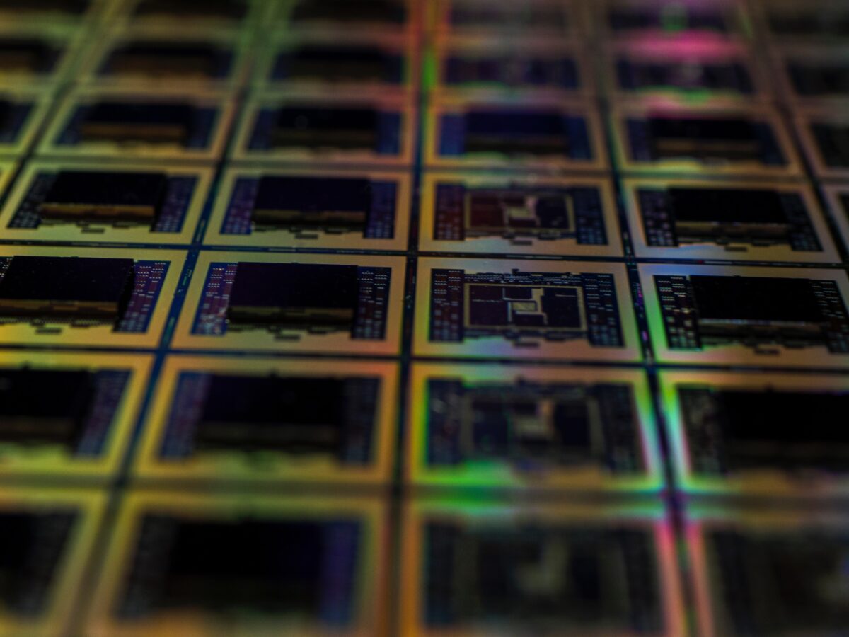
Transistors are a vital, ubiquitous electronic component. Their main function is to switch or amplify the electrical current in a circuit, and a modern device like a smartphone can contain between 2 and 4 billion transistors.

So that’s some modern context, but have you ever wondered when the transistor was invented? Or what it looked like?

Pre-transistor technology

Going way back to when Ohm’s Law was first discovered in 1820s, people had been aware of circuits and the flow of current. As an extension of this, there was an awareness of conductors.

Following on from this, semiconductors accompanied the birth of the AC-DC (alternating current – direct current) conversion device, the rectifier, in 1874.

Two patents were filed in the 20s and 30s for devices that would have been transistors if they had ever reached past the theoretical stage. In 1925 Julius Lilienfeld of Austria-Hungary filed a patent, but did not end up releasing any papers regarding his research on the field-effect transistor, and so his discoveries were ignored.

Again, in 1934 German physicist Oskar Heil’s patent was on a device that, by applying an electrical field, could control the current in a circuit. With only theoretical ideas, this also did not become the first field effect transistor.

The invention of transistors

The official invention of a working transistor was in 1947, and the device was announced a year later in 1948. The inventors were three physicists working at Bell Telephone Laboratories in New Jersey, USA. William Shockley, John Bardeen and Walter Brattain were part of a semiconductor research subgroup working out of the labs.

One of the first attempts they made at a transistor was Shockley’s semiconductor triode, which was made up of three electrodes, an emitter, a collector and a large low-resistance contact placed on a block of germanium. However, the semiconductor surface trapped electrons, which blocked the main channel from the effect of the external field.

Despite this initial idea not working out, the issue was solved in 1946. After spending some time looking into three-layer structures featuring a reversed and forward-biased junction, they returned to their project on field-effect devices in a year later in 1947. At the end of that year, they found that with two very close contact junctions, with one forward biased and one reverse biased, there would be a slight gain.

The first working transistor featured a strip of gold over a triangle of plastic, finely cut with a razor at the tip to create two contact points with a hair’s breadth between them and placed on top of a block of germanium.

The device was announced in June of 1948 as the transistor – a mix of the words ‘transconductance’, ‘transfer’ and ‘varistor’.

The French connection

At the same time over the water in France, two German physicists working for Compagnie des Freins et Signaux were at a similar stage in the development of a point contact device, which they went on to call the ‘transistron’ when it was released.  

Herbert Mataré and Heinrich Welker released the transistron a few months after the Bell Labs transistor was announced but was engineered completely without influence by their American counterpart due to the secrecy around the Bell project.

Where we are now

The first germanium transistors were used in computers as a replacement for their predecessor vacuum tubes, and transistor car radios were produced all within only six years of its invention.

The first transistor was made with germanium, but since the material can’t withstand heats of more than 180˚F (82.2˚C), in 1954 Bell Labs switched to silicon. Later that year Texas Instruments began mass-producing silicon transistors.

First silicon transistor made in 1954 by Bell Labs, then Texas Instruments made first commercial mass produced silicon transistor the same year. Six years later in 1960 the first in the direct bloodline of modern transistors was made, again by Bell Labs – the metal-oxide-semiconductor field-effect Transistor (MOSFET).

Between then and now, most transistor technology has been based on the MOSFET, with the size shrinking from 40 micrometres when they were first invented, to the current average being about 14 nanometres.

The latest in transistor technology is called the RibbonFET. The technology was announced by Intel in 2021, and is a transistor whose gate surrounds the channel. The tech is due to come into use in 2024 when Intel change from nanometres to, the even smaller measuring unit, Angstrom.

There is also other tech that is being developed as the years march on, including research into the use of 2D materials like graphene.

If you’re looking for electronic components, Lantek are here to help. Contact us at sales@Lantekcorp.com to order hard-to-find or obsolete electronic components. You can also use the rapid enquiry form on our website https://www.cyclops-electronics.com/

Categories
Electronic Components

Latest electronic component factory openings

Latest electronic component factory openings

We’ve all heard about the shortages in standard components like semiconductors and chips. Cars, phones and computers, items we use every day, are no longer being produced at the speedy rate we’ve come to expect. The cause of this shortage is, in part, due to the COVID-19 pandemic.

To combat this shortage many electronic component manufacturers have announced the opening or development of new factories. This is especially noticeable in Europe and America, where production has often been outsourced to Asia in the past.

So who are the latest companies expanding operations, and how much are they spending? Check out our quick run-down of factories and when they should open:

Company: Intel

Location: Ohio, USA

Product: Chips

Completion date: 2025

Cost: $20 billion (£14.7 billion)

The latest, and possibly greatest, announcement on our list comes from Intel. The corporation revealed in January that they would be committing to building two chip manufacturing plants in New Albany, Ohio. The move is said to be due to supply chain issues with Intel’s manufacturers in Asia, and should boost the American industry with the creation of at least 3,000 jobs. Construction should begin this year.

Company: Samsung Electronics

Location: Texas, USA

Product: Semiconductors

Completion date: 2024

Cost: $17billion (£12.5billion)

The household name announced late last year that they would begin work on a new semiconductor-manufacturing plant in Taylor, Texas. The Korean company stated the project was Samsung’s largest single investment in America, and is due to be operational by the middle of 2024.

Company: Infineon

Location: Villach, Austria

Product: Chips

Completion date: 2021

Cost: 1.6 billion (£1.3 billion)

After being in construction since 2018, Infineon’s Austrian plant became operational in September last year. The chip factory for power electronics, also called energy-saving chips, on 300-millimeter tin wafers began shipping three months ahead of schedule in 2021, and its main customer base will be in the automotive industry.

Company: Northvolt

Location: Gdańsk, Poland

Product: Batteries

Completion date: 2022

Cost: $200 million (£148 million)

The Swedish battery manufacturer is expanding its operations with a new factory in Poland. While initial operations are supposed to begin this year producing 5 GWh of batteries, it hopes to further develop to produce 12 GWh in future. Northvolt has also just begun operations at its new battery factory in Skellefteå in Sweden.

Company: Vingroup

Location: Hà Tĩnh, Vietnam

Product: Batteries

Completion date: 2022

Cost: $174 million (£128 million)

The Vietnamese electric vehicle manufacturer is due to start production at its new factory later this year, where it will produce lithium batteries for its electric cars and buses. The factory will be designed to produce 10,000 battery packs per year initially, but in a second phase the manufacturer said it will upgrade to 1 million battery packs annually. VinFast, a member of Vingroup, is also planning on expanding operations to America and Germany.

Company: EMD Electronics

Location: Arizona, USA

Product: Gas and chemical delivery systems

Completion date: 2022

Cost: $28 million (£20.7 million)

The member of the multinational Merck Group is expanding operations with the construction of a new factory in Phoenix, Arizona, to manufacture equipment for its Delivery Systems & Services business. The factory is due to be operational by the end of the year, and will produce GASGUARD and CHEMGUARD systems for the company.

A bright future

These electronic component factory openings signal a great increase in business, and will aide in the easing of the component crisis. But it will take a while for these fabs to be operational.

Can’t wait? Lantek is there for all your electronic component needs. We have 30 years of expertise, and can help you where other suppliers cannot. Whether it’s day-to-day or obsolete electronic components, contact us today at sales@lantekcorp.com, or use the rapid enquiry form on our website.