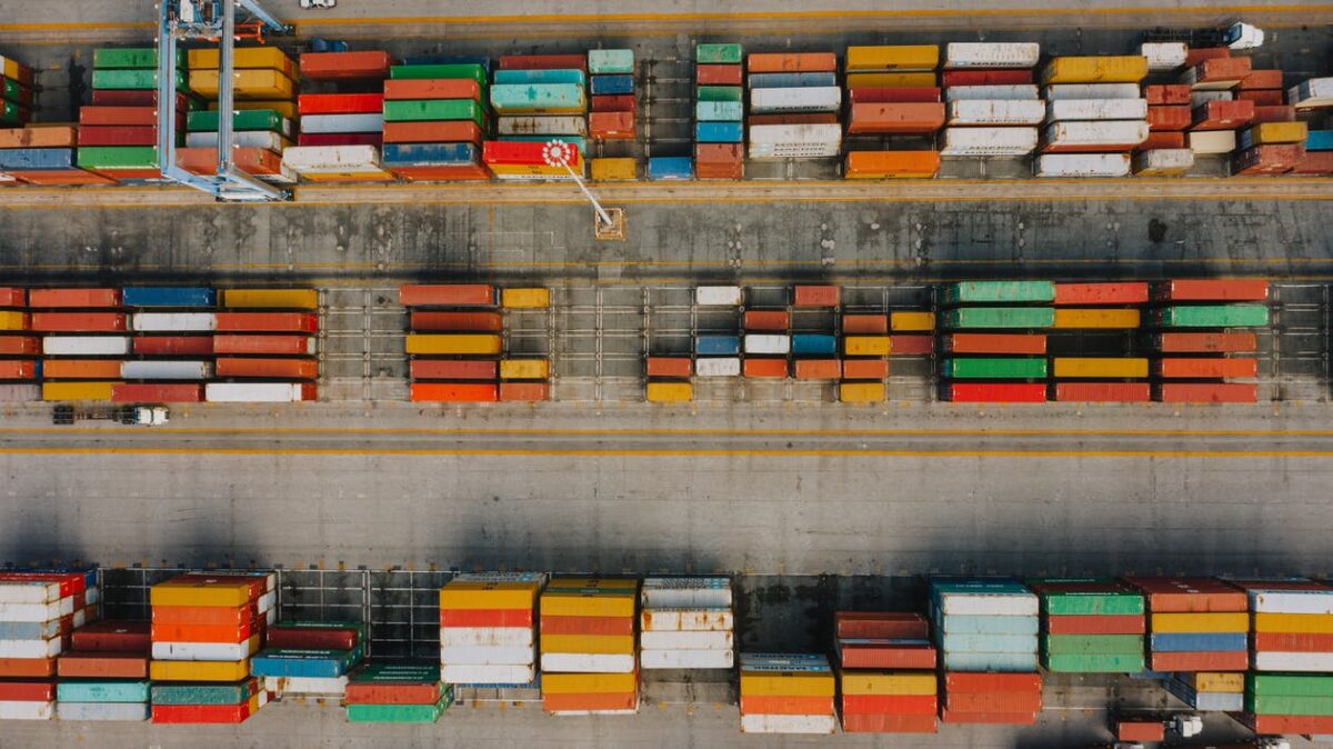
Supply chain adaptability
Connectivity within our supply chain is a positive thing. It has given us access to resources from all over the world, boosting production and sourcing. However, covid and other factors have highlighted the risk that comes with having a globally connected supply chain.
If covid was the only concern, though, the supply chain would have recovered by now. The general increase in supply and demand has also left the industry struggling to catch up.
If there is a disruption to one area of the supply chain, this is then passed down the line to customers. At every step of the supply chain, the delays are exacerbated and impacts the economy.
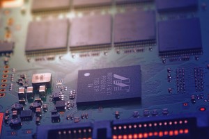
Connectivity and interdependence have always been essential in the electronics industry, whether it is relying on other countries for materials or working with international foundries on production.
Certain countries had, and some still have, covid-related restrictions in place to stop the potential spread. This means that plants in those countries have had difficulty keeping up with demand. As one of the biggest exporters of electronics is also in this position, some countries are choosing to transition away from working with them.
Some large companies have already made the decision to move their base of operations to mitigate this risk in the future. This has the potential to massively shift industry dynamics and encourage other businesses to make similar moves.
Funding is being allocated by some governments to facilitate nearshoring or reshoring of companies, which would bolster the supply chain. Many countries, including the US, UK and India, are increasing the budget and support of domestic chip production. There will be several ongoing effects from this, including an increase in skilled workers, R&D and more in-house production.
Although this would be beneficial there would still need to be materials sourced from countries including places in turmoil. Even relocating a percentage of the supply chain will not resolve these sourcing conundrums. However, it would reduce shipping times and customs charges for the finished product, especially if production is closer to customers.
As much as it would be beneficial to reshore or nearshore production, it comes with certain risks. The cost of labour varies largely depending on location, as does the number of skilled workers. Additionally, the delay or difficulties associated with moving production halfway around the world will also be numerous.
Many countries have put measures and funds in place to encourage moves, but financial aid will only reach so far.
More than a long-term static solution, the supply chain needs to be flexible and adaptable. Supply, demand, and the world in general is very volatile right now. As such, suppliers and manufacturers will have to alter their ways of working accordingly.
Lantek has the rare advantage of being able to source electronic components from all over the world. This, combined with our keen eye and careful inspection processes, means we can find and supply the components you need.
Call today on 1-973-579-8100 to speak to a member of our sales team, or contact us at sales@lantekcorp.com
Disclaimer: This blog is meant purely for educational or informational purposes and is in no way instructional.