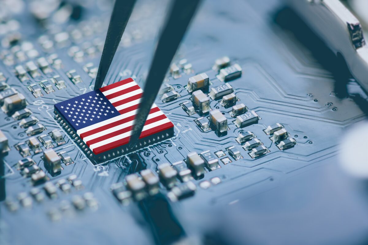

New US India semiconductor partnership
The US recently formed a partnership with India with an aim to cooperate in several industries, including semiconductor production. This is
hoped to be a very fruitful partnership, especially since the increase in restrictions between China and the US.
Recent changes
More companies have been investing in India in recent years, including Vedanta-Foxconn, PSMC and Micron Technology. Partly thanks to new government incentive schemes, companies are trying to move manufacturing into the country. More are expected to follow as India increases its funding for semiconductor manufacturing.
The Indian Government and related parties have announced several incentives for incoming companies. One of the largest was that there would be a 50% waiver on the cost of establishing a fab.
The US and Indian Semiconductor Associations (SIA and IESA respectively) have also formed a taskforce to strengthen collaboration. The taskforce plans to assess the country’s readiness to sustain a semiconductor market and make recommendations to increase its presence in the
supply chain.
But it hasn’t been easy. Many incoming companies have mentioned difficulties with a lack of infrastructure, difficult regulations, and other struggles.
The competition
India could also potentially help in the sourcing of minerals for semiconductor production. Currently much of the world’s supply (72%)
comes from China, which could prove troublesome soon enough.
However, India is apparently abundant in 49 critical and non-fuel minerals that are used in the industry according to a report by the Council on Energy, Environment and Water (CEEW) and the Ministry of Science and Technology.
Work away
Another potential benefit to the States is the new ‘friend-shoring’ location it has unlocked. While the Chips Act attempts to move much of the
process to domestic, this won’t be entirely achievable.
The high cost of labor and the lack of highly-skilled employees within the field will prove challenging. In a collaboration with India, however, it would provide a manufacturing location with manageable labor costs. It could also pave the way for highly-skilled professionals from India
to work in the US.
There are hopes that this collaboration is the next big milestone for the countries since the 2016 nuclear power agreement.
A different kind of partnership
We have a steadfast relationship with all of our customers, thanks to the trust and reliability we are known for. Lantek Corporation can fulfil
all your electronic part needs, all you need to do is contact us. We’re available at sales@lantekcorp.com or call us on 1-973-579-8100.