Semiconductors in space
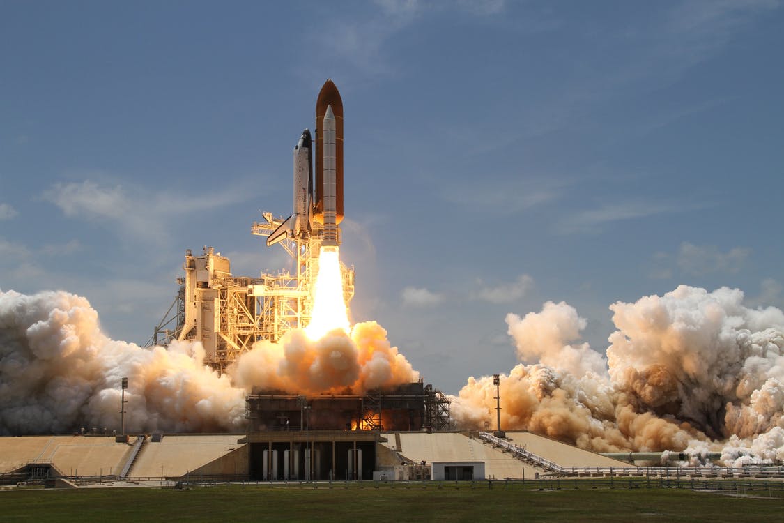
Blast off
A post about semiconductors being used in space travel would be the perfect place to make dozens of space-themed puns, but let’s stay down to earth on this one.
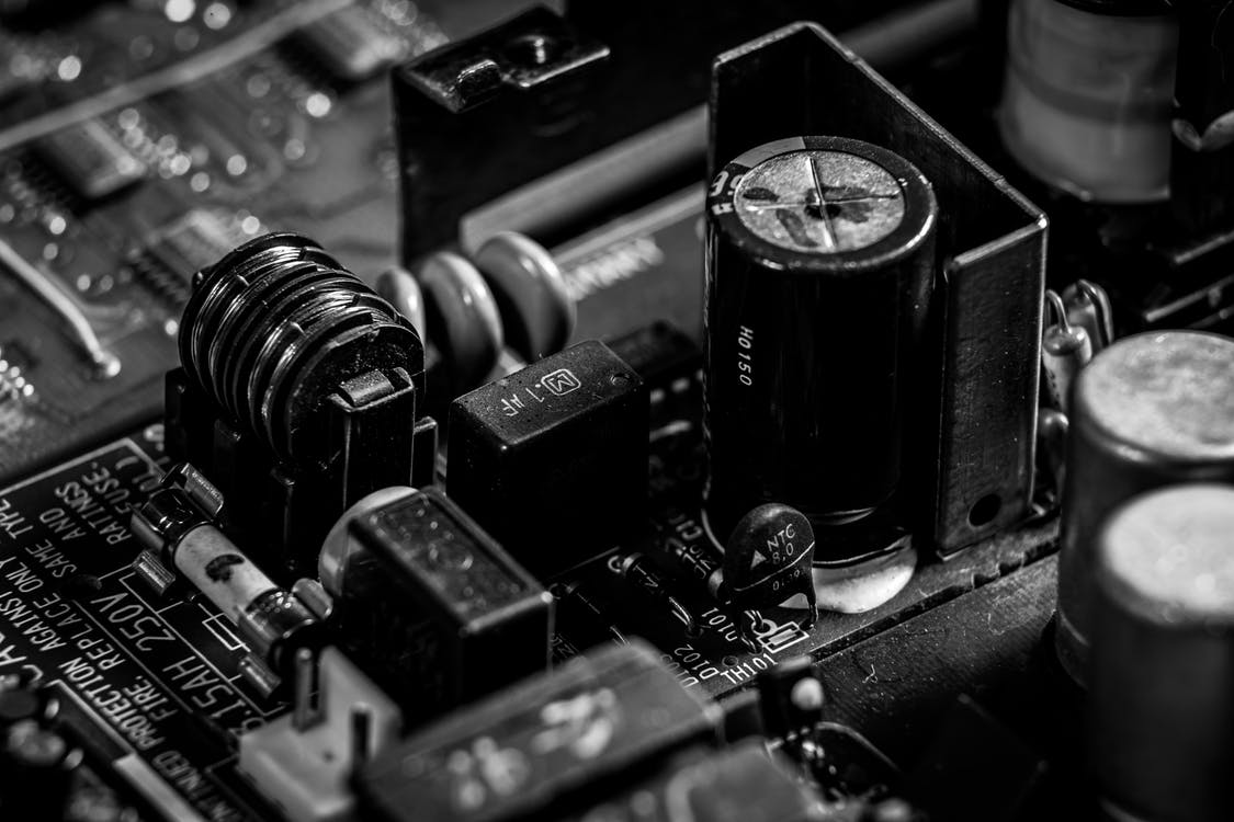
There are around 2,000 chips used in the manufacture of a single electric vehicle. Imagine, then, how many chips might be used in the International Space Station or a rocket.
Despite the recent decline in the space semiconductor market, it’s looking likely that in the next period there will be a significant increase in profit.
What effect did the pandemic have?
The industry was not exempt from the impact of the shortage and supply chain issues caused by covid. Sales decreased and demand fell by 14.5% in 2020, compared to the year-on-year growth in the years previous.
Due to the shortages, many companies within the industry delayed launches and there was markedly less investment and progress in research and development. However, two years on, the scheduled dates for those postponed launches are fast approaching.
The decline in investment and profit is consequently expected to increase in the next five years. The market is estimated to jump from $2.10 billion in 2021 all the way up to $3.34 billion in 2028. This is a compound annual growth rate (CAGR) of 6.89%.
What is being tested for the future
In the hopes of ever improving the circuitry of spaceships there are several different newer technologies currently being tested for use in space travel.
Some component options are actually already being tested onboard spacecrafts, both to emulate conditions and to take advantage of the huge vacuum that is outer space. The low-pressure conditions can emulate a clean room, with less risk of particles contaminating the components being manufactured.
Graphene is one of the materials being considered for future space semiconductors. The one-atom-thick semiconductor is being tested by a team of students and companies to see how it reacts to the effects of space. The experiments are taking place with a view to the material possibly being used to improve the accuracy of sensors in the future.
Two teams from the National Aeronautics and Space Administration (NASA) are currently looking at the use of Gallium Nitride (GaN) in space too. This, and other wide bandgap semiconductors show promise due to their performance in high temperatures and at high levels of radiation. They also have the potential to be smaller and more lightweight than their silicon predecessors.
GaN on Silicon Carbide (GaN on SiC) is also being researched as a technology for amplifiers that allows satellites to transmit at high radio frequency from Earth. Funnily enough, it’s actually easier to make this material in space, since the ‘clean room’ vacuum effect makes the process of epitaxy – depositing a crystal substrate on top of another substrate – much more straightforward.
To infinity and beyond!
With the global market looking up for the next five years, there will be a high chance of progress in the development of space-specialised electronic components. With so many possible advancements in the industry, it’s highly likely it won’t be long before we see pioneering tech in space.
To bring us back down to Earth, if you’re looking for electronic components contact Lantek today to see what they can do for you. Email us at sales@lantekcorp.com or use the rapid enquiry form on our website.