Categories
component shortage

How electronics shortages may affect Christmas – The known and the unknown

How electronics shortages may affect Christmas

Christmas is just around the corner, and while many shortages have calmed there are some that persist and will have an impact on the usual holiday festivities.

Despite reports that shortages are ending, more than half of semiconductor industry leaders are expecting them to continue into 2023.

There are shortages that we have been prepared for as the months counted down to the holidays. However, other shortages may catch some unawares.

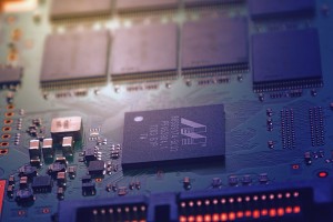
Much of the news regarding shortages has revolved around the difficulty producing new, smaller nodes. These are the semiconductors going into new consumer electronics, often purchased as Christmas gifts.

What was expected:

As semiconductor shortages persist, next-gen consumer electronics will be in limited supply. Demand always spikes around the holidays, as consumers prepare for the gifting season. But some will be out of luck since electronics have also been affected by the shortages.

While consumer electronics, including smartphones, smart home devices, and games consoles have become slightly more stable, there will still be shortages in the face of holiday buying and events like Black Friday.

This also affects the manufacture of new cars, both fuel and electricity-powered models. Many car companies have lowered the number of vehicles produced. Although they haven’t been able to meet the increased demand, semiconductor shortages mean they cannot produce more.

What you didn’t expect:

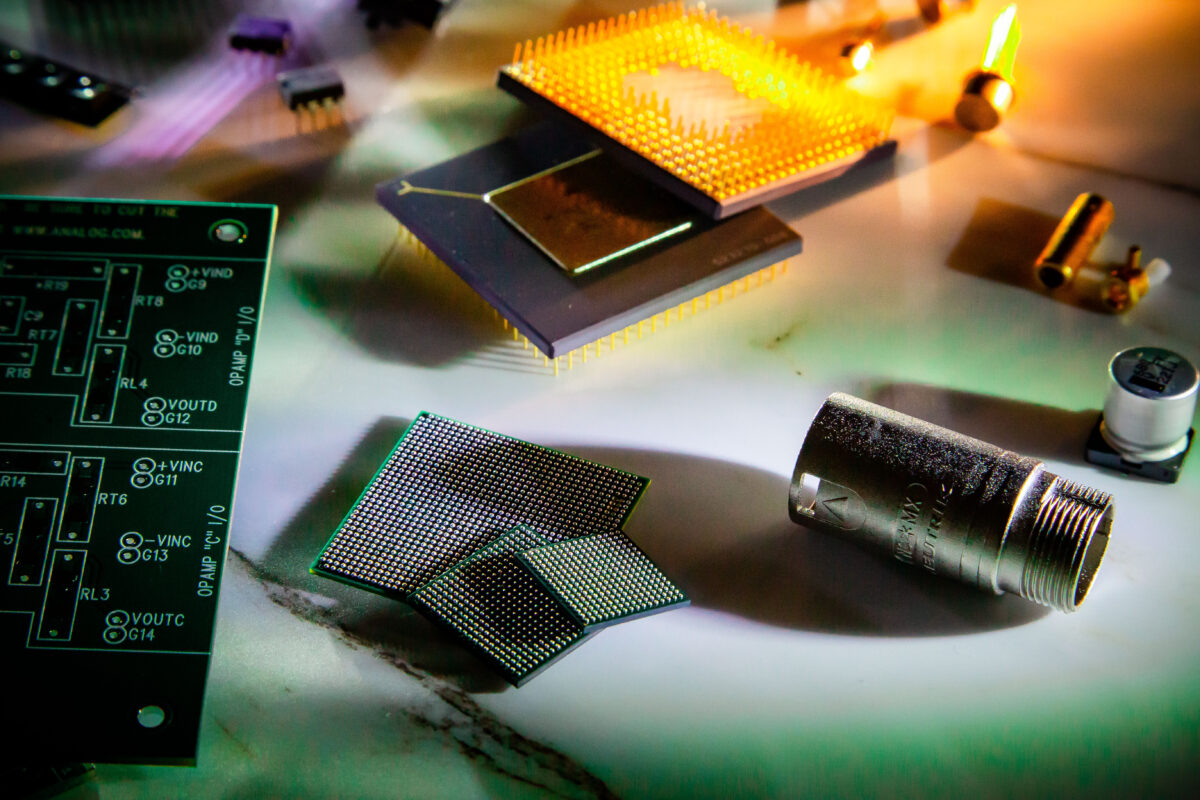
New electronic components are not the only ones that are in short supply. Older components and obsolete electronic parts have also become scarcer.

Embedded flash microcontrollers are one component that has long been used in automotive manufacture. Most of the ones used are still using older nodes, like 90nm. So while new cars are being affected, older cars in need of repair will also be impacted.

Industrial electronics are also at risk due to shortages, since they similarly rely on legacy nodes. Traditionally these would be the more stable of options for electronic components. However, the reserves that have taken years to build are now being drained.

Although companies are planning on investing in legacy nodes, the shortages are expected to last until at least 2024, if not 2025.

The shortages show no sign of stopping, and manufacturers will be dealing with the effects of it for years to come. There are surely plenty of electronic components and markets affected that have not been mentioned here, so this overview is by no means exhaustive.

What to expect

As shortages persist, there’s no better time to get in touch with us.

Lantek Corp has an extensive supply of day-to-day and obsolete electronic components. If you have been struggling to source components elsewhere, Lantek Corp is there for you.

Let us provide your Christmas miracle this year, call us on 1-973-579-8100 or email us at sales@lantekcorp.com

Categories
Electronic Components

Should we be investing in GaN fabs?

Should we be investing in GaN fabs?

The wide bandgap semiconductor Gallium Nitride (GaN) has many advantageous properties, but it has been difficult to scale up production.  

During such an invigorating period in the industry, silicon semiconductors have been in massive demand. And in short supply. It has not been the best time to consider switching to a new wafer material. Not that there ever will be a quiet moment in this sector.

Where it all beGaN

GaN has only really been in the picture since the mid-90s, when its top uses were military. Since then it has seen growth, with a revenue of $1 billion in 2020 according to Strategy Analytics. Silicon wafer revenue, in comparison, was $11.2 billion. GaN is still a small fry.

Despite GaN production being a much smaller endeavour currently, there are several companies currently manufacturing GaN devices. GaN is currently used for power electronic devices thanks to their high electron mobility and high breakdown voltages.

A survey was undertaken by Microwave Journal, wherein they contacted major GaN suppliers around the world. Of the 8 that responded, there were 36 variants available, with gate lengths ranging between 0.5ɥm to 40nm. The GaN variants included GaN-on-SiC, GaN on Si and GaN on diamond substrates.

The potential future of semiconductors

We’ve talked before about how GaN could be a future replacement for the aging silicon semiconductors. This would not only benefit consumers because of its fast performance, but would also benefit the environment.

The first and most obvious factor, is that with more efficient semiconductors less of them would be required. GaN requires less raw material and because of the reduced size there can be more units per wafer.

Aside from this, the actual manufacturing emissions for GaN are much lower. Gallium metal is a by-product of aluminium smelting, and nitrogen is readily available in the atmosphere. GaN, then, has a minimal carbon footprint and is easily sourced.

If GaN could be used globally, it could make a difference against climate change, more than silicon or silicon carbide. It is also non-toxic and includes no conflict materials. GaN power IC devices can also be manufactured using already-established CMOS processing equipment.

It’s not GaNna be easy…

So GaN could well be a great alternative for silicon in years to come, however the problem comes with up-scaling production and transitioning. Changing the semiconductor material would undoubtedly incur several design and logistical changes, and would cause disruptions and delays.

Some industry experts have suggested investing in mega-fabs to produce GaN-on-Si wafers for manufacturers. This would help even out the disparity between GaN and silicon stock, and encourage more manufacturers to produce GaN devices.

It’s estimated that the GaN-based power IC management market will grow by about 70% each year from 2020 to 2026. This is just one use of GaN, but demonstrates how profitable the material may be in the future.

Lantek has a huge range of stock which includes both brand new electronic components and obsolescent stock. Whatever you may need Lantek can provide it. Get in touch with us today to see what we can do for you! Contact us on sales@lantekcorp.com or call us on 1-973-579-8100

This blog is purely for entertainment and informational purposes, it is in no way instructional.

Categories
Electronic Components

Electronics to measure climate change

Electronics to measure climate change

Semiconductors are being used to track and combat the effects of climate change. Their use could help scientists better understand the impact and process global warming has on the planet.

Climate change and global warming are topics that are often discussed in modern society, both by governments and individuals alike. There are certain industries that are thought to be larger contributors to the current situation. However, the electronics industry may be able to help rather than hinder the battle against climate change.

Accelerometers

These electronic components have been used to measure the effects of climate change through trees.

Accelerometers measure the vibration or acceleration of motion of a structure. Inside is a piezoelectric material, which makes an electrical charge proportional to the force caused by the motion.

The electronic device can be used for a variety of things, from spaceships to smartphones. But recently, researchers have been tying them to trees.

These so-called ‘tree fitbits’ can track the timing of tree activities like blooming or the leaves changing. Two ash trees in East Boulder were fitted with high-resolution accelerometers which tracked how they responded to the changing seasons.

The hope is that in the future tree phenology (the study of periodic events in biological life cycles) can be studied in relation to climate change. The accelerometers measured the amount that the trees swayed and the high frequency vibrations of the tree itself. This helps scientists track the phases of the tree (phenophases) as the seasons progress.

The data means that the start and end of each season for the tree, for example flowering in spring, can be measured and compared to data from previous years. The differences can be indicative of climate change and could be used as a warning sign.

Sensors

Miniscule sensors inspired by dandelion seeds could be scattered to track climate change indicators as well. The sensors were produced by a team from the University of Washington in Seattle. The electronic devices are made from polyimide films, and were manufactured using a laser-powered tool. Throughout its structure there are tiny holes, which aids it in floating like a dandelion seed.

The benefit of these tiny sensors means researchers can reach dangerous places without putting themselves at risk. Tracking temperature, humidity and other environmental signals across a large area would be beneficial to climate change research.

On board there are tiny solar panels and a capacitor that can store energy overnight when conditions are not optimal.

Indicators of change?

The future of the planet is not set in stone, and electronic devices can make a difference. Both in prediction and prevention, electronics are aiding us in our efforts. Lantek can provide electronic components for you to make your own change. Trust Lantek to supply you, contact us on sales@lantekcorp.com or 1-973-579-8100

This blog is purely for entertainment and informational purposes, it is in no way instructional.

Categories
Electronic Components

Supply chain adaptability

Supply chain adaptability

Connectivity within our supply chain is a positive thing. It has given us access to resources from all over the world, boosting production and sourcing. However, covid and other factors have highlighted the risk that comes with having a globally connected supply chain.

If covid was the only concern, though, the supply chain would have recovered by now. The general increase in supply and demand has also left the industry struggling to catch up.

If there is a disruption to one area of the supply chain, this is then passed down the line to customers. At every step of the supply chain, the delays are exacerbated and impacts the economy.

Connectivity and interdependence have always been essential in the electronics industry, whether it is relying on other countries for materials or working with international foundries on production.

Certain countries had, and some still have, covid-related restrictions in place to stop the potential spread. This means that plants in those countries have had difficulty keeping up with demand. As one of the biggest exporters of electronics is also in this position, some countries are choosing to transition away from working with them.

Some large companies have already made the decision to move their base of operations to mitigate this risk in the future. This has the potential to massively shift industry dynamics and encourage other businesses to make similar moves.

Funding is being allocated by some governments to facilitate nearshoring or reshoring of companies, which would bolster the supply chain. Many countries, including the US, UK and India, are increasing the budget and support of domestic chip production. There will be several ongoing effects from this, including an increase in skilled workers, R&D and more in-house production.

Although this would be beneficial there would still need to be materials sourced from countries including places in turmoil. Even relocating a percentage of the supply chain will not resolve these sourcing conundrums. However, it would reduce shipping times and customs charges for the finished product, especially if production is closer to customers.

As much as it would be beneficial to reshore or nearshore production, it comes with certain risks. The cost of labour varies largely depending on location, as does the number of skilled workers. Additionally, the delay or difficulties associated with moving production halfway around the world will also be numerous.

Many countries have put measures and funds in place to encourage moves, but financial aid will only reach so far.

More than a long-term static solution, the supply chain needs to be flexible and adaptable. Supply, demand, and the world in general is very volatile right now. As such, suppliers and manufacturers will have to alter their ways of working accordingly.

Lantek has the rare advantage of being able to source electronic components from all over the world. This, combined with our keen eye and careful inspection processes, means we can find and supply the components you need.

Call today on 1-973-579-8100 to speak to a member of our sales team, or contact us at sales@lantekcorp.com

Disclaimer: This blog is meant purely for educational or informational purposes and is in no way instructional.

Categories
Electronic Components

Process nodes and transistor density

Process nodes and transistor density

There are regular news articles published claiming that the smallest ever process node has been produced. We hear all the time about how small chips are becoming. But how can we measure this progress and does size really matter?

Moore’s Law

The concept of Moore’s Law, loosely, is that the number of transistors in a microchip increases as the size decreases. Originally, when Gordon Moore observed this in 1965, it was thought that the number of transistors would double every two years, but this rapid rate has definitely slowed.

Even so, there is still a constant increase in the number of transistors that can fit on an IC. In 1971, 6 years after the advent of Moore’s Law, there were around 2.3 thousand transistors on a single chip. This sounds like a lot, but we can now fit hundreds of millions onto one.

Nowadays, as it probably always was, it is a race between manufacturers to produce the smallest, most advanced chips. And with the advancement of manufacturing technology, the stakes are higher than ever.

Process nodes

The main method of measuring electronic component progress now is through process nodes. This is the term used for the equipment used for semiconductor wafer production. It describes the minimum repeatable half-pitch (half the distance between two identical features on a chip) of a device. It seems, though, that even this node measurement is no longer accurately used, according to some sources.

Some recent node announcements come from big players in the industry, including Intel, Samsung and TSMC. Taiwan’s largest semiconductor company, TSMC, recently announced that it would be converting its 3nm process node into 1.4nm. Critics, however, were not sure how possible this would be.

Samsung also recently revealed its plans to start manufacturing 2nm process chips in 2025. Additionally, Intel is planning on producing 1.8nm chips in late 2024. Part of the process of developing smaller process nodes is changing the technology involved in production.

What is the measure of a chip?

The method of measuring chips by process nodes is not entirely accurate and can be quite ambiguous. Some people have suggested chip density within the chip would be a better indicator of advancement.

While companies compete to develop the smallest process, some companies are fitting more chips onto bigger nodes. To put it in perspective, Intel’s 7nm process has 237 million per millimetre squared. In comparison, TSMC’s 5nm chip has only 171 million per millimetre squared.

So, although certain chips may have a smaller process node, it doesn’t necessarily reflect how advanced the chip actually is. Intel often uses density to describe its chips, because that is much more beneficial to them.

It’s a process

The question is, should all chips be measured this way instead of in process nodes? If process nodes aren’t accurate to their original definition, the measurements don’t indicate of the highest power chips out there. This might be confusing to consumers when choosing a manufacturer.

It will become increasingly difficult to measure in process nodes as chips get increasingly smaller. Many manufacturers are already making plans for when they begin to measure in Angstrom rather than nanometres. If the changeover from one measurement type to another was not confusing enough, if the measurement method is inaccurate, it may get very complicated.

Apparently, though, transistor count can be just as inaccurate because there is no standard way of counting them. The number of transistors on a single chip design can vary by 33-37% which is quite substantial.

The final node

Unfortunately, there’s no definitive answer on how to measure the advancement of chips anymore. Moore’s Law is far from dead, but is very much up to interpretation these days. Those purchasing or sourcing chips will have to have their wits about them.

For those sourcing chips, contact Lantek. We can source day-to-day or hard-to-find components with ease and can guarantee our customers the best price. Get in touch via sales@lantekcorp.com or call us on 1-973-579-8100 

Categories
Electronic Components

One week until Electronica!

One week until Electronica!

This year one of the largest electronics trade fairs in the world is taking place in Munich, Germany.

Lantek founder has been attending Electronica since it first began, so the convention has always been a highlight of our calendar. We have met many clients and partners through the connections provided to us by Electronica.

The convention is focusing on the promotion of sustainability this year. Bringing the industry together in one location with the aim of “Driving Sustainable Progress”, Electronica hopes to show the role the world that electronics will help, not hinder, sustainability.

The previous Electronica in 2020 was purely virtual, but having hundreds of exhibitors back in Messe München, spread over 13 halls, will be an event to remember.

 In 2018 there were more than 81,000 visitors to the trade fair from 101 countries. 3,124 exhibitors attended the event, we’re hoping for an even more enthusiastic turnout this time around.

In 2021 there was a 9.8% increase in industry revenue from the previous year, at €200 billion, which is astounding progress during the pandemic.

Electronica will have a supporting program full of knowledge and professional talks. During conferences experts will analyse market activity.

The convention has been held every other year since 1964, and has continually grown and evolved over the years.

In the final week leading up to the trade fair, we want to organise meetings with all our clients who are also attending. Whether you are a returning or new customer, we want to show you what Lantek can do for you.

We have the expertise and drive to go the extra mile for you. Whether you are looking to buy or sell, Lantek has a solution for you.

Whether you are a returning customer or are completely new to Lantek, we want to meet you. If you are attending Electronica you can book an appointment with our staff to discuss your needs at Eventbrite now.

Categories
Electronic Components

Keeping clean and going green for Electronica

Keeping clean and going green for Electronica

The Lantek staff are busy preparing for the biggest event in the Lantek calendar: Electronica. This is the time for us to meet our customers, both returning and new. But this year, we are making sure we’re doing things the clean, green way.

Since Covid, we are paying special attention to the hygiene services we provide. There will be hand sanitiser and wipes available on our stand, along with gloves and masks.

It is more important than ever to ensure we are environmentally conscious, and to that end we are taking steps to minimise our environmental impact.

As we are shipping our goods from the UK to Germany, we are making sure we are using much less disposable packaging. As far as possible we have reduced our packing and will be reducing the total volume of goods shipped to avoid unnecessary emissions.

The goods we are shipping to Electronica are also greener than in previous years. One of the OEM rewards we are giving out to our customers is the Rocketbook.

This notebook is a fusion of traditional handwriting and digitisation. The Rocketbook is a paper notebook with a QR code on each page. When paired with the phone app you can scan the code, upload pages of writing and digitize the text. Once it is uploaded, you can clear the page of the notebook and use it again.

This reusable approach to a traditional tool is something we at Lantek are passionate about. We are looking forward to sharing this innovation with our customers!

We are also taking other steps to go green for Electronica. The disposable products that we would have taken in the past are being replaced with recyclable alternatives, like paper cups for drinks instead of plastic.

With only 2 weeks until Electronica preparation is in full swing for the event. We can’t wait to see you all there!

Come visit the Lantek team in Hall 4, stand 126. In the meantime, you can always contact us on 1-973-579-8100 , or email us at sales@lntekcorp.com

Categories
Electronic Components

The benefits of flexible electronics

The benefits of flexible electronics

Flexible electronics is an area of study that has come on in leaps and bounds in recent years and is an area of interest for many electronics companies. Liquid metal circuits are being researched as a potential step-up for wearable tech and biomedical devices.

At present, there are certain elements that make the advancement of flexible electronics difficult. One of these elements is the conductive material inside. If a rigid material like copper is used in flexible circuitry, it may break.

Some researchers are looking into the use of conductive threads, like those made out of carbon nanotubes. Others are taking a different approach and developing liquid metal circuits.

Quicksilver

Liquid metal used for circuits has not been a popular concept for a long time, mostly due to the fame (or infamy) of mercury. Mercury is a liquid at room temperature, but is highly toxic and couldn’t be used in electronics for safety reasons. Gallium, however, is beginning to look like a viable alternative.

While Gallium has a slightly higher melting point than mercury, it is not toxic and can conduct heat and electricity. The metal forms an oxide layer in the open air and this was viewed as a disadvantage in the past. Now, though, it could be advantageous when creating flexible circuitry.

Soft robots

Flexible electronics could have a number of uses in everyday life, and one hoped use is for soft robotics. With soft robots food could be handled safely without the risk of cross-contamination. It also opens up a wealth of possibilities for deep-sea exploration and specimen collection.

In a different area, soft robotics could have biomedical uses. Wearable technology, drug delivery devices and artificial organs are all potential utilisations of stretchable, human-mimicking electronics.

Soft robotics are already being used for prosthetic limbs. In 2020 a prosthetic hand was created for amputees, with functioning fingers and a moving thumb. Although in the very early stages of development, the prototype could pave the way for life-changing robotics in the future.

Virtually real

Aside from the more medical or safety-focused applications, there could be more recreational uses too. The use of soft robotics in conjunction with VR could make for an even more immersive user experience.

Stretching or twisting a mesh of gallium wires by it will change the electrical current running through them. At the moment this is still being researched, but it could be used for VR in the future. If gallium mesh was used in gloves, it could detect the pressure applied and translate it into VR.

Whether it’s for recreational, medical or safety purposes, exploring the use of liquid metal circuits and researching their potential could be greatly beneficial to the electronics industry, and the industries that come after it.

Lantek can provide a substantial range of electronic components, and we’re experts at sourcing hard-to-find components when others cannot. If you’re looking for components, whether they’re obsolete or day-to-day, choose Lantek as your supplier. Contact us now on 1-973-579-8100 or send us an email at sales@lantekcorp.com

This blog is purely for entertainment and informational purposes, it is in no way instructional.

Categories
Electronic Components

3D printing of electronic components

3D Printing of Electronic Components

We talk a lot about the ways modern technology are a benefit to the electronics industry. There’s no better example of this than the ability to 3D print electronic components.

Print preview

The first 3D printer was invented in the 1980s, and used a technique called stereolithography (SLA). You might recognise the term from photolithography, a process used in the manufacturing of semiconductor wafers. Stereolithography is slightly different, it uses a laser to harden layers of photopolymer successively in a pre-defined shape. Photolithography is for etching patterns onto semiconductor wafers.

SLA is still the most commonly-used method of 3D printing. There are, however, other methods that have come into use, including digital light processing and liquid crystal display.

With the printing of components or circuits that can conduct electricity, special inks that contain conductive nanomaterials are required.

The process

First, a digital model of the desired component is required. This is referred to as a Computer Aided Design, or CAD model. Then a base layer of the material, usually thermoplastics, is formed using fused deposition modelling (FDM).

After this a trace is created, which is the little web of wiring you can see on a regular PCB. These traces need to be much thicker on a 3D-printed board because the nano-inks naturally carry more resistance than copper.

Once this is complete, the additional components of the board are added in layers until it is finished.

Why use 3D printing?

The process of retooling an entire factory setup versus uploading a different design to a single machine are vastly different. Retooling can be a costly and painstaking process, especially if you are manufacturing on a small scale or just prototyping.

The flexibility that comes with 3D printing is also an advantage. Where regular machinery may have limitations, 3D printing could have significantly fewer.

There would also be a reduction in the waste produced by the process. Most of the time, boards are manufactured and then the excess material is cut away. With 3D printing there would be remarkably less waste produced as it only prints what is needed.

3D printing of electronic components is currently used for small batches or for rapid prototyping, but in the future it could easily be used for more complex components and larger batches.

Just a reminder

Although Lantek does not specialise in 3D printers, we do specialise in electronic components of all kinds, and can supply stock as and when you need it. Make Lantek your electronic component supplier.

This blog is meant for informational purposes only and is in no way instructional.

Categories
Electronic Components

The price of semiconductor equipment is increasing

The price of semiconductor equipment is increasing

The price of chip manufacturing is increasing. From skyrocketing raw material prices to continual high demand for semiconductors, it/ is an expensive business right now. Semiconductor manufacturing prices are also on the rise.

Global manufacturers are announcing price hikes to combat the expected rise in inflation, passing the cost onto the customer.

Is reshoring reassuring?

Aside from the supply chain issues and raw material shortages, the drive for reshoring will drive up the cost and demand of semiconductor manufacturing equipment.

In both the US and the UK, new legislation is in the works to provide funding for the electronics industry. It comes alongside a push to reduce reliance on semiconductors sourced from Asia, especially powerhouses like Taiwan and China.

The Chips Acts

In the west’s new legislation, funding and incentives are offered to domestic and international companies looking to build fabs. One such company was TSMC itself, which was rumoured last year to be opening a branch in Germany.

While these grants and investments will go some way to covering the cost of new semiconductor manufacturing equipment, it will only be part of the massive price manufacturers pay.

A new challenger

This may not be the only international development affecting the price increases of semiconductor equipment. New competitors are throwing their proverbial hat in the semiconductor manufacturing ring. One of the countries that is beginning to manufacture more is India.

As the US and Europe are already heavy-hitters in the industry, India will have to make hefty investments into manufacturing. Bulk-buying machinery and technology for facilities will mean more demand, and distributors putting on a bigger price tag. Taiwanese manufacturer Foxconn announced it would be setting up a fab in the country.

Other costs

The cost of making the semiconductor manufacturing equipment also comes into play. As companies are persuaded to move west, the cost of their manufacturing will increase. Many companies based in the east have access to cheaper labour but European and US labour costs will be higher.

Outside of Asia, in areas that are reshoring, there will also be the struggle of finding highly qualified employees. Since there was no need for skilled individuals when there were no fabs, there is a gap in the industry. It will take some time to catch up with industry standards of education.

Kit up

As the chip shortages continue, there’s no guarantee when the cost increase of semiconductor manufacturing equipment might slow down. As with all things, we’ll have to wait and see.